
Data transmission circuit and data transmission method with two transmission modes

Inactive Publication Date: 2008-05-06
RENESAS ELECTRONICS CORP
View PDF4 Cites 7 Cited by
  • Summary
  • Abstract
  • Description
  • Claims
  • Application Information

AI Technical Summary

Benefits of technology

[0038]Another object of the present invention is to provide efficient construction of a data transmission circuit supporting a plurality of transmission modes.
[0056]A data transmission method according to the present invention is a data transmission method having a first transmission mode and a second transmission mode, the data transmission method outputting output data in accordance with input data, including, in the first transmission mode, a step of selectively setting a plurality of switching elements to on state in accordance with an impedance control signal; a step of controlling a constant current driver based on the input data; and a step of outputting output data in accordance with an output of the constant current driver and on-state resistance of the switching elements; and, in the second transmission mode, a step of selecting selected switching elements from the plurality of switching elements in accordance with an impedance control signal; and a step of outputting data by turning on / off the selected switching elements in accordance with the input data. This method allows transmitting data in a suitable condition in any of the plurality of transmission modes.

Problems solved by technology

However, the above output buffer has the followings problems.
It is therefore impossible to control both output impedance and a slew rate.
However, reduction of a number of transistors reduces the load capacitance of the prebuffer 106.
There is thus a problem that the slew rate of an output waveform differs between control codes.
However, if an output slew rate is controlled by the capacitor array as with the case with output impedance control, a capacitance appears differently between the feedback capacitor and the gate electrode of a drive transistor due to bias voltage dependency, which makes control not easy.
However, the conventional CMOS push / pull circuit and the circuit described in Japanese Patent Application Laid-Open No. 2000-59201 are difficult to design to attain stable signal transmission in high-speed data transmission such as newly offered by the USB 2.0 standard.
The above conventional output buffer circuit, however, cannot meet the requirement.

Method used


Image

  • Data transmission circuit and data transmission method with two transmission modes
  • Data transmission circuit and data transmission method with two transmission modes
  • Data transmission circuit and data transmission method with two transmission modes

Examples


Embodiment Construction

[0063]In the following, a preferred embodiment of the present invention will be explained in detail with reference to the drawings.

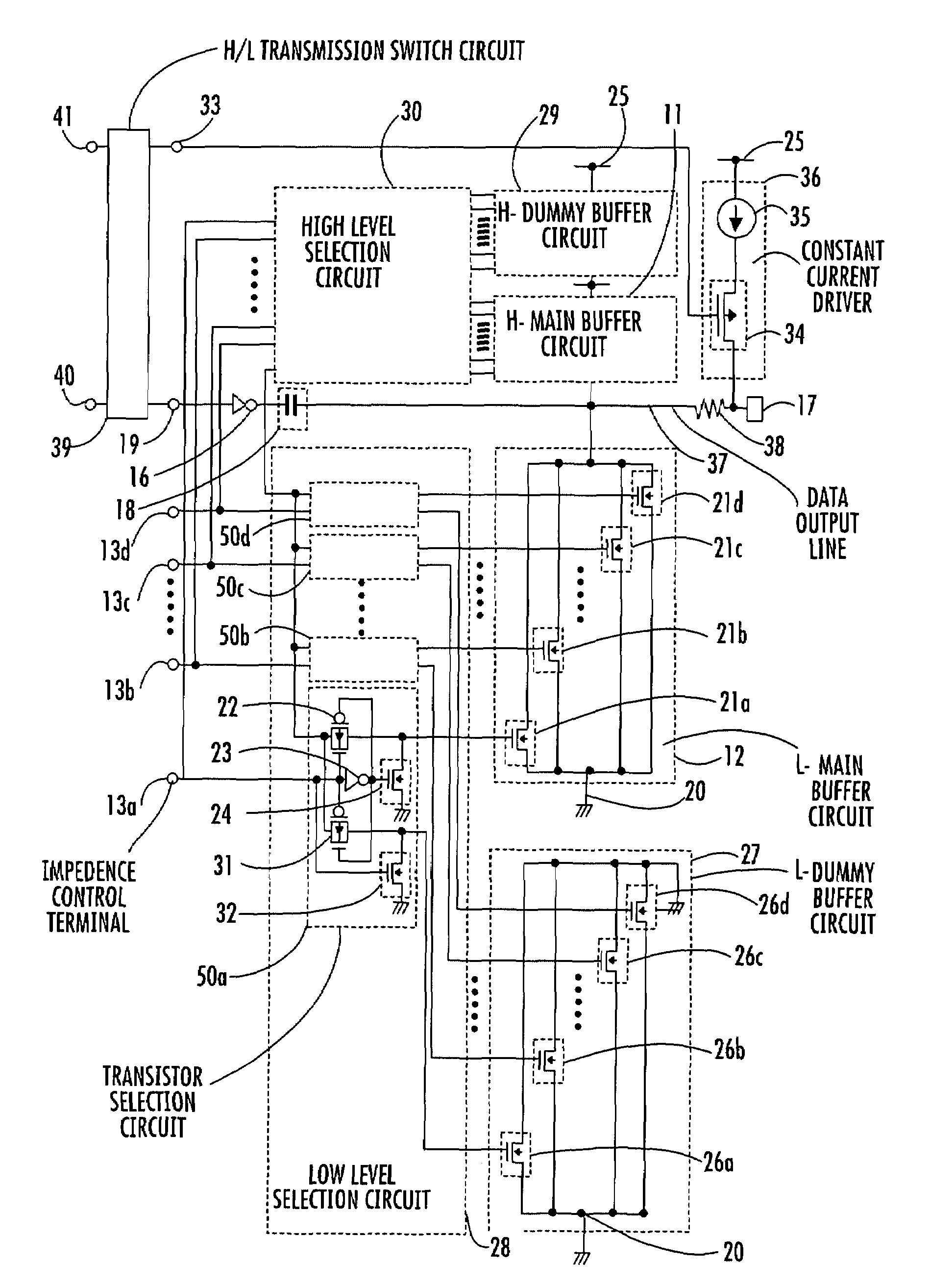
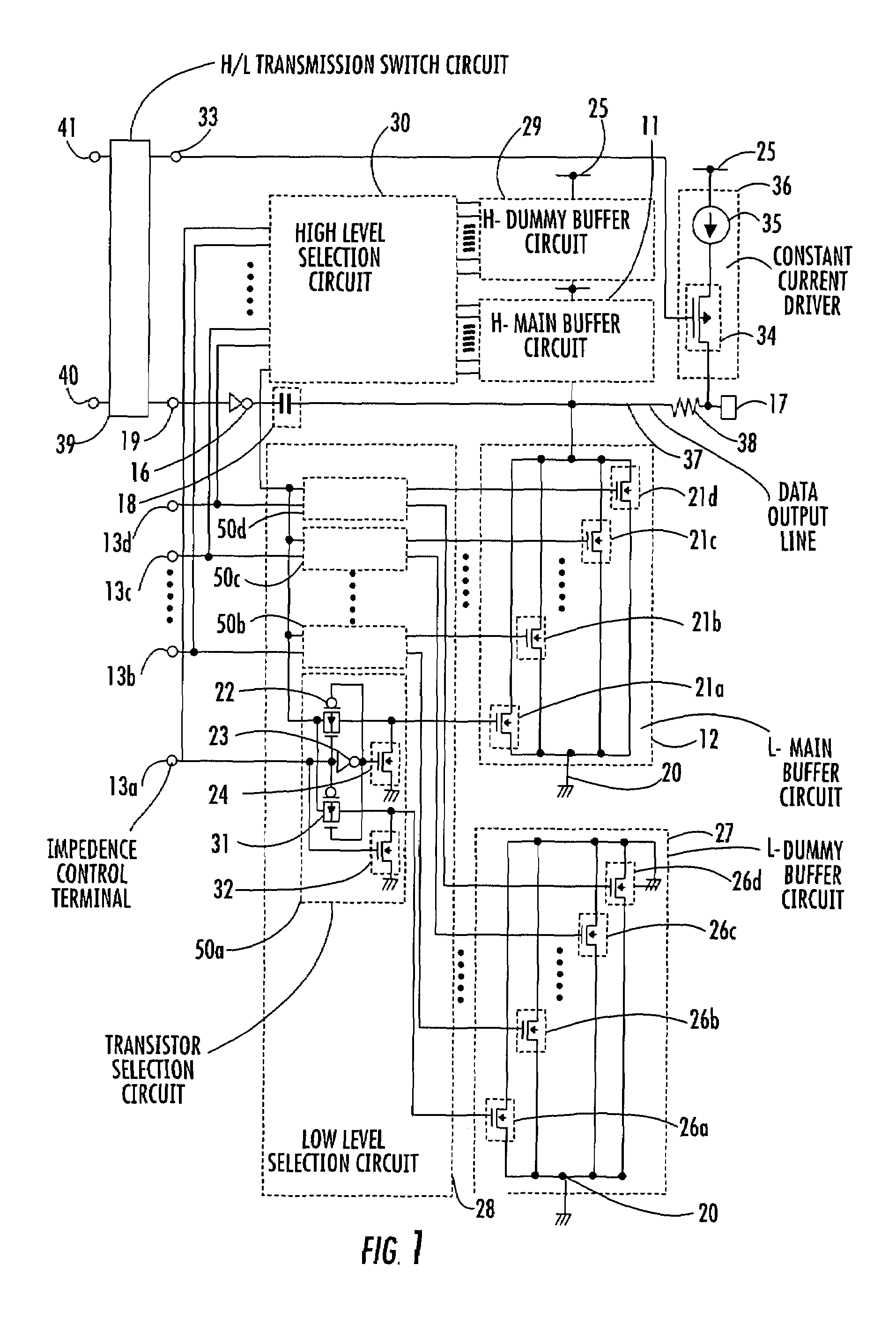
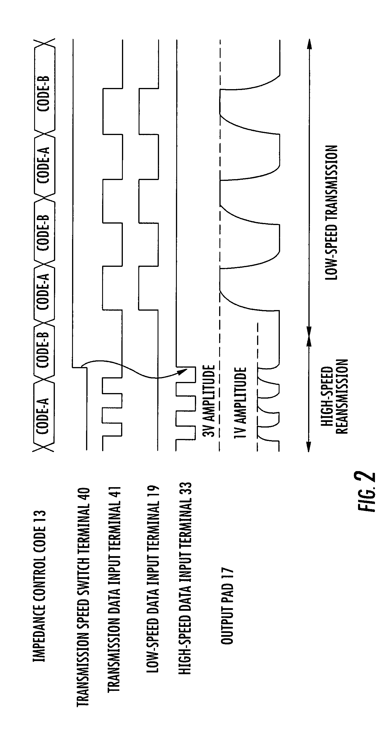
[0064]First, the configuration of data transmission circuit according to a preferred embodiment of the present invention will be described hereinbelow with reference to FIG. 1. FIG. 1 schematically shows a configuration example of a data transmission circuit according to the present embodiment, comprising an output buffer circuit employing a CMOS push / pull type constant voltage driver for low-speed transmission, and an output buffer circuit employing a constant current driver for high-speed transmission. The figure shows a substantial part of the data transmission circuit. The data transmission circuit according to the present embodiment is effective when applied to the output buffer of a USB 2.0 controller, for example. The data transmission circuit uses a constant current driver in higher speed data transmission with the transfer rate of 480 Mbps, and ...


PUM


Abstract

In a data transmission circuit according to the present invention, selection circuits alternately switch between transistors of a main buffer and transistors of a dummy buffer. In high-speed data transmission, a H / L transmission switch circuit outputs high-speed data to a constant current driver and outputs a selection signal for inputting a control signal to the main buffer to a selection circuit. In low-speed data transmission, on the other hand, the H / L transmission switch circuit outputs a selection signal for inputting a control signal to the main buffer in accordance with the low-speed data to the selection circuit. The H / L transmission switch circuit controls an input of the control signal to the main buffer in accordance with the selection signal.

Description

BACKGROUND OF THE INVENTION[0001]1. Field of the Invention[0002]The present invention relates to a data transmission circuit and a data transmission method. More specifically, the present invention relates to a data transmission circuit and a data transmission method in which data is input and output in a plurality of transmission modes.[0003]2. Related Background Art[0004]Conventionally, a computer and a peripheral device have been connected using an interface for peripheral devices such as a serial interface and a parallel interface. Recently, a universal serial bus (USB), IEEE1394 and other serial interfaces to connect a variety of peripheral devices have come into wide use to integrate and standardize interfaces.[0005]Out of the need of the recent information society for high-speed communication of large volumes of data, USB 2.0 standard offering a faster data transfer rate than the conventional USB 1.x standard such as USB 1.0 standard (the standard of USB Implements Forum or U...

Claims


Application Information

Patent Timeline
IPC IPC(8): H03K19/094H03K19/0175H04L12/28H04L25/02
CPCH04L25/0278H04L25/028H03K19/0175
Inventor IWASAKI, TADASHI
Owner RENESAS ELECTRONICS CORP
Features
  • Generate Ideas
  • Intellectual Property
  • Life Sciences
  • Materials
  • Tech Scout
  • Unparalleled Data Quality
  • Higher Quality Content
  • 60% Fewer Hallucinations
Learn More