
Method and apparatus to prevent high voltage supply degradation for high-voltage latches of a non-volatile memory

a non-volatile memory and latch technology, applied in static storage, digital storage, instruments, etc., can solve the problems of affecting low-voltage operation, increasing threshold voltage vt, and limited current capability of high-voltage generators, and achieve high impedance and prevent leakage current

Active Publication Date: 2008-05-06
SONRAI MEMORY LTD
View PDF8 Cites 10 Cited by
  • Summary
  • Abstract
  • Description
  • Claims
  • Application Information

AI Technical Summary

Benefits of technology

"The present invention provides a non-volatile memory with high-voltage latches that have a high impedance in series with a second CMOS inverter during a HIGH-VOLTAGE WRITE mode of operation to limit leakage current. The memory also includes a switching circuit that provides a low impedance in series with the second CMOS inverter during the standby mode of operation to minimize leakage current. The invention also provides a method of limiting leakage current in the high-voltage latches during data writing."

Problems solved by technology

The high-voltage generator typically has limited current capability and excessive leakage currents in the some of the high-voltage latches may load down the generator so much as to cause the high-voltage level to be less than what is required for proper writing of data bits into the memory cells of the non-volatile memory.
Changing process parameters for fabrication of the pull-down NMOS transistor 24 may reduce leakage; but this can cause its threshold voltage Vt to increase and adversely affect low-voltage operation.

Method used


Image

  • Method and apparatus to prevent high voltage supply degradation for high-voltage latches of a non-volatile memory
  • Method and apparatus to prevent high voltage supply degradation for high-voltage latches of a non-volatile memory
  • Method and apparatus to prevent high voltage supply degradation for high-voltage latches of a non-volatile memory

Examples


first embodiment

of the Invention

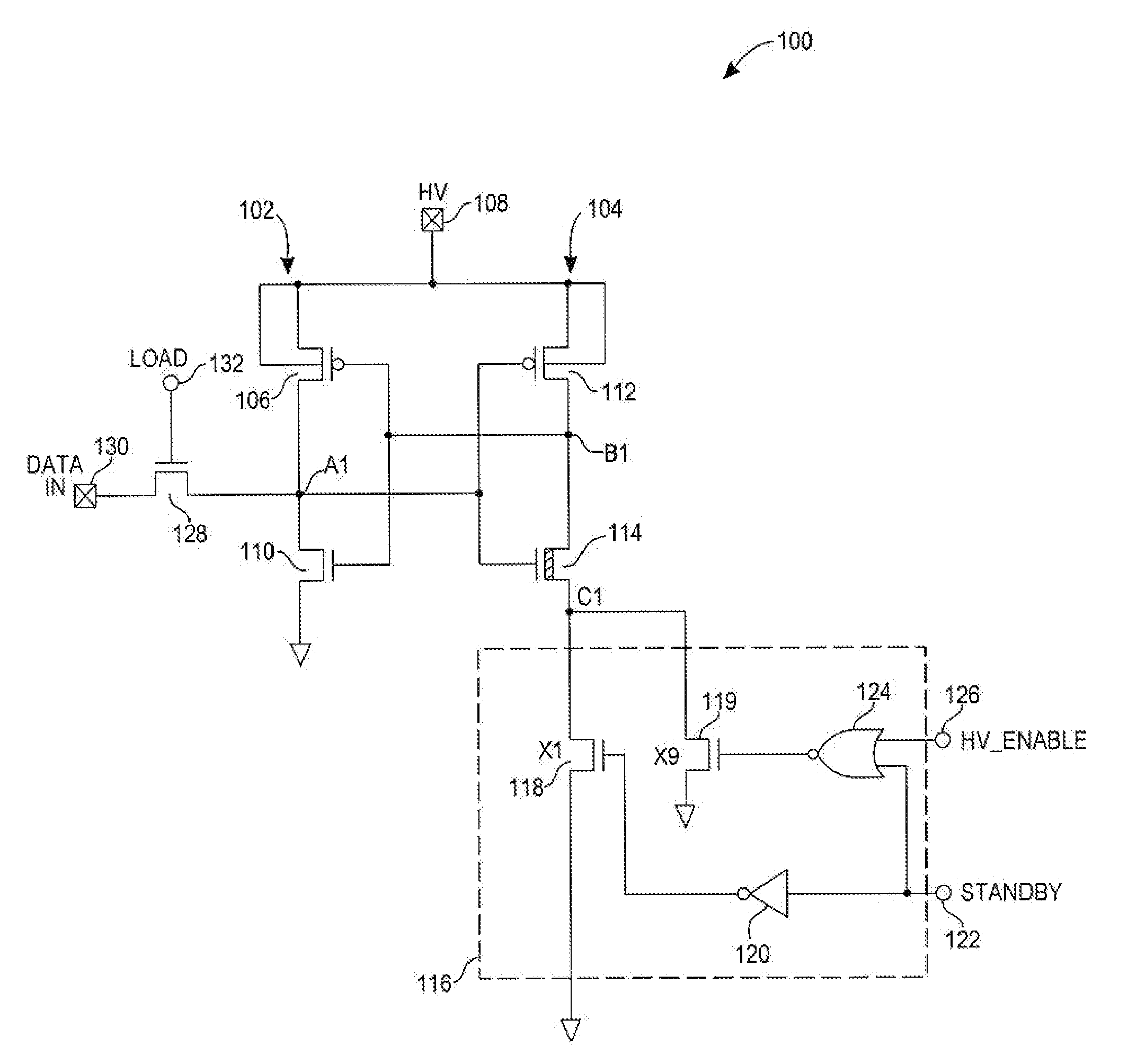
[0033]FIG. 3 is a circuit diagram of a first embodiment of a high voltage latch circuit 100 that includes a first CMOS inverter circuit 102 and a second CMOS inverter circuit 104. The first CMOS inverter circuit 102 includes a first pull-up PMOS transistor 106 that has a drain connected to a HV node 108 and a source connected to a latch input node A1. The first CMOS inverter circuit 102 also includes a first pull-down NMOS transistor 110 that has a drain connected to the latch input node A1 and a source connected to ground. The gates of the first pull-up PMOS transistor 106 and the first pull-down NMOS transistor 110 are connected together.

[0034]The second CMOS inverter circuit 104 includes a second pull-up PMOS transistor 112 that has a drain connected to the HV node 108 and a source connected to a data storage output node B1. The second CMOS inverter circuit 104 includes a second NMOS pull-down transistor 114 that has a drain connected to the data storage output no...

second embodiment

of the Invention

[0045]FIG. 5 is a circuit diagram of a second embodiment of a high voltage latch circuit 200, where components similar to those of FIG. 3 have the same reference characters, such as the first CMOS inverter circuit 102 and the second CMOS inverter circuit 104. The first CMOS inverter circuit 102 includes the first pull-up PMOS transistor 106 that has a drain connected to the HV node 108 and a source connected to a latch input node A2. The first CMOS inverter circuit 102 also includes the first pull-down NMOS transistor 110 that has a drain connected to the latch input node A2 and a source connected to ground. The gates of the first pull-up PMOS transistor 106 and the pull-down NMOS transistor 110 are connected together.

[0046]The second CMOS inverter circuit 104 includes a second pull-up PMOS transistor 112 that has a drain connected to the HV node 108 and a source connected to a data storage output node B2. The second CMOS inverter circuit 104 includes a second pull-d...

third embodiment

of the Invention

[0055]FIG. 6 is a circuit diagram of a third embodiment of a high voltage latch circuit 300, where similar components have the same reference characters, such as the first CMOS inverter circuit 102 and the second CMOS inverter circuit 104. The first CMOS inverter circuit 102 includes a first pull-up PMOS transistor 106 that has a drain connected to a HV node 108 and a source connected to a latch input node A3. The first CMOS inverter circuit 102 also includes a first pull-down NMOS transistor 110 that has a drain connected to the latch input node A3 and a source connected to ground. The gates of the first pull-up PMOS transistor 106 and the first pull-down NMOS transistor 110 are connected together.

[0056]The second CMOS inverter circuit 104 includes a second pull-up PMOS transistor 112 that has a drain connected to the HV node 108 and a source connected to a data storage output node B3. The second CMOS inverter circuit 104 includes a second pull-down NMOS transistor ...


PUM


Abstract

An improved cross-coupled CMOS high-voltage latch that is used for storing data bits to be written to memory cells of a non-volatile memory is provided with a switching circuit that, during writing of data bits into the memory cells of the latch, provides a high series impedance between one leg of the latch and ground to limit leakage current. A large number of latches are connected in parallel and their accumulated leakage currents are limited by the switching circuit to prevent overload of a high-voltage generator, such as a charge pump circuit, for the high-voltage latch, so that data can be properly written in the memory cells of the non-volatile memory.

Description

TECHNICAL FIELD[0001]The present invention relates to high-voltage data latches that are used writing data into a non-volatile memory and, more particularly, to apparatus and a method for limiting leakage current drawn from a high voltage supply or generator, such as an on-chip charge pump circuit.BACKGROUND ART[0002]A latch is used to store data bits to be written into pre-selected memory cells of a non-volatile memory. Except when data bits are being written into the memory cells, the latch is normally supplied with a low-voltage power supply, such as, for example, 3 volts or less. During a write mode of operation, the latch is supplied with a high voltage of 7-15 volts, as required for writing data into the non-volatile memory cells. A single non-volatile memory chip may contain a large number, for example, 512 or more high-voltage latch circuits. These latch circuits are typically called high-voltage latch circuits, although a high voltage supply is only required for write opera...

Claims


Application Information

Patent Timeline
Patent Type & Authority Patents(United States)
IPC IPC(8): G11C7/00
CPCG11C7/1078G11C16/10G11C7/1087G11C2207/2227G11C7/00G11C16/00
Inventor CHAN, JOHNNYSON, JINSHU
Owner SONRAI MEMORY LTD
Learn More