Reduction of hillocks prior to dielectric barrier deposition in Cu damascene

a dielectric barrier and hillock technology, applied in the direction of coating, plasma technique, cleaning of hollow articles, etc., can solve the problems of high electrical resistance and/or shorting, affecting the performance of the interconnect structure, etc., and achieve the effect of minimizing energy and minimizing thermal budg

Inactive Publication Date: 2008-05-13
APPLIED MATERIALS INC
View PDF25 Cites 11 Cited by
  • Summary
  • Abstract
  • Description
  • Claims
  • Application Information

AI Technical Summary

Benefits of technology

[0012]Unwanted hillocks arising in copper due to formation of overlying barrier layers may be significantly reduced by optimizing various process parameters, alone or in combination. A first set of process parameters may be controlled to pre-condition the processing chamber in which the barrier layer is deposited. A second set of process parameters may be controlled to minimize energy to which a copper layer is exposed during removal of CuO prior to barrier deposition. A third set of process parameters may be controlled to minimize the thermal budget after removal of the copper oxide.

Problems solved by technology

The growth and presence of hillocks 108a can create issues regarding performance of the interconnect structure, such as elevated electrical resistance and / or shorting.

Method used


Image

  • Reduction of hillocks prior to dielectric barrier deposition in Cu damascene
  • Reduction of hillocks prior to dielectric barrier deposition in Cu damascene
  • Reduction of hillocks prior to dielectric barrier deposition in Cu damascene

Examples


Embodiment Construction

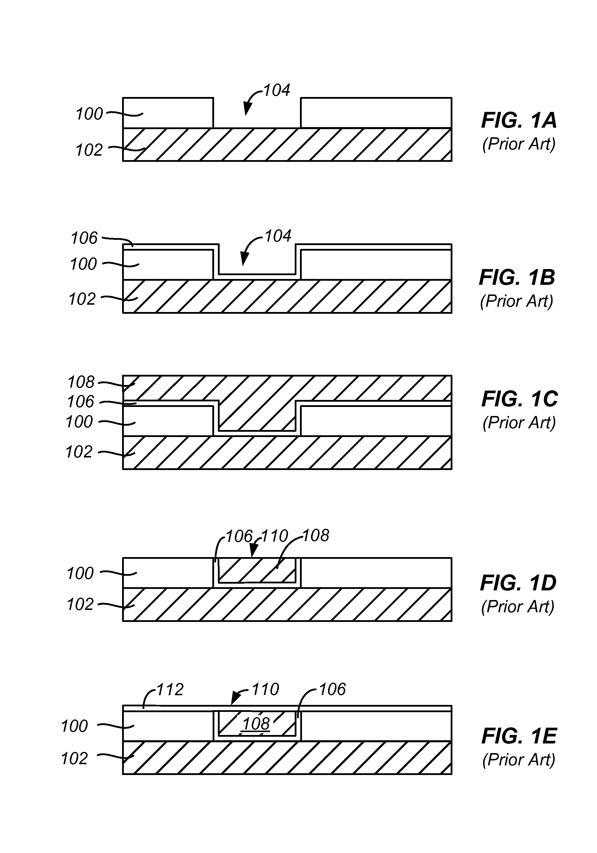
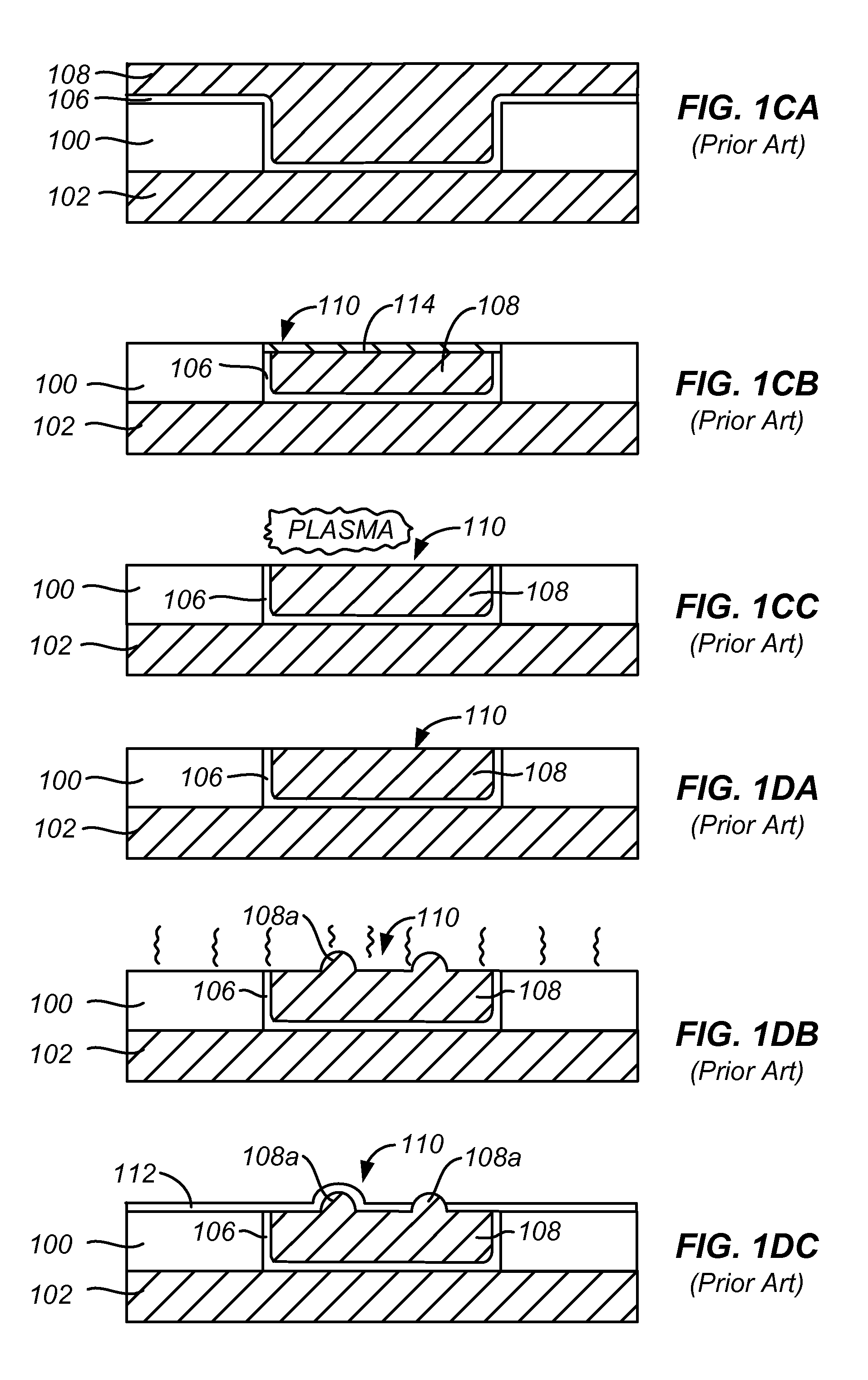
[0032]Unwanted formation of hillocks in copper layers during the fabrication of semiconductor devices may be reduced in accordance with embodiments of the present invention by carefully controlling a number of process parameters, alone or in combination. A first set of process parameters may be controlled to pre-condition the barrier layer deposition chamber prior to its receiving a wafer bearing a copper layer. A second set of process parameters may be controlled to minimize the energy to which the copper layer is exposed during removal of copper oxide prior to deposition of the barrier layer. A third set of process parameters may be controlled to minimize the thermal budget that the copper layer is exposed to after removal of the copper oxide. Control over each of these sets of parameters is discussed in detail below.

I. Reduction of Hillock Formation in Copper Layers

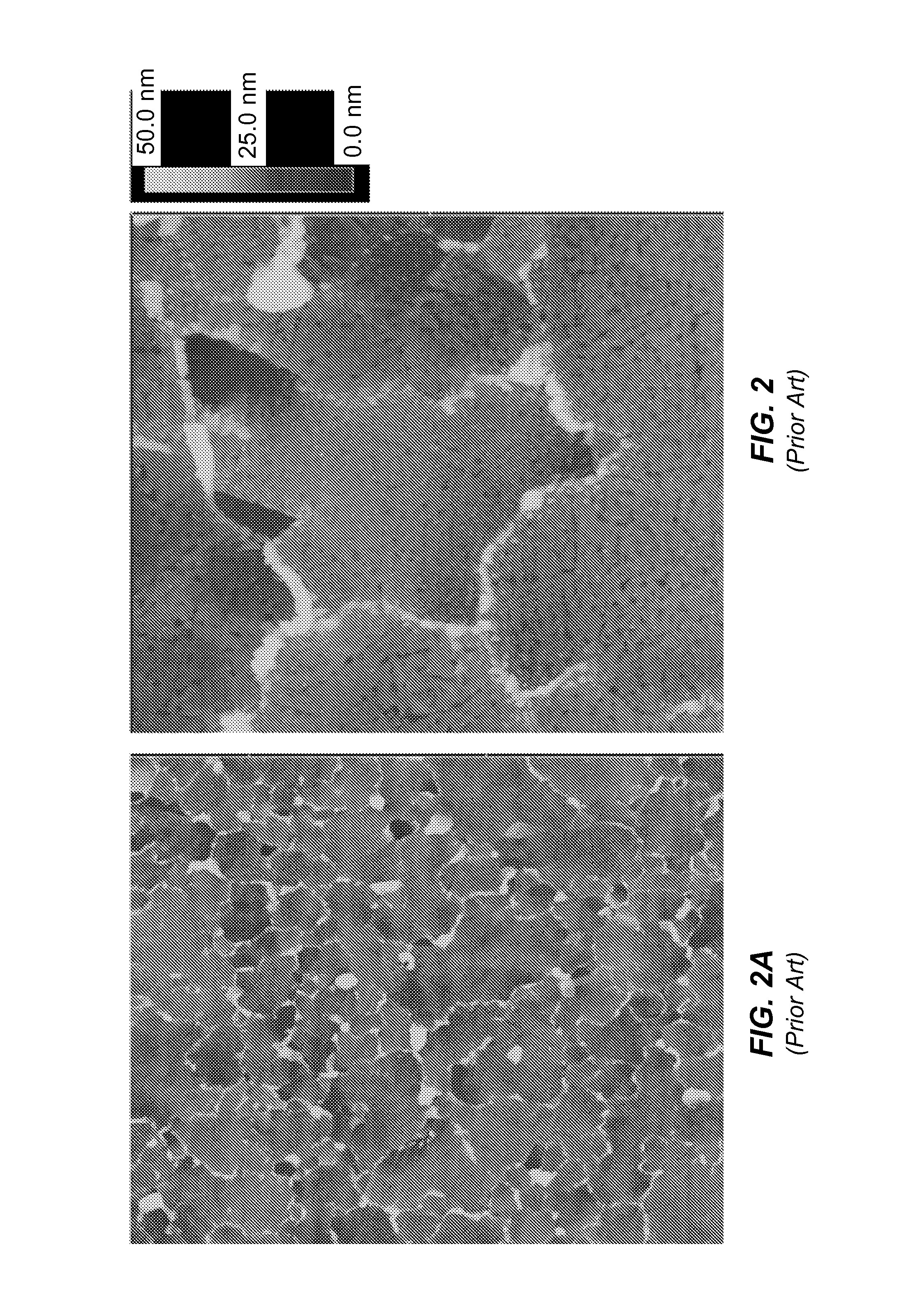
[0033]Research has indicated that the formation of hillocks in copper layers may be attributable to diffusion of cop...


PUM

PropertyMeasurementUnit
temperatureaaaaaaaaaa
pressureaaaaaaaaaa
pressureaaaaaaaaaa

Abstract

Unwanted hillocks arising in copper layers due to formation of overlying barrier layers may be significantly reduced by optimizing various process parameters, alone or in combination. A first set of process parameters may be controlled to pre-condition the processing chamber in which the barrier layer is deposited. A second set of process parameters may be controlled to minimize energy to which a copper layer is exposed during removal of CuO prior to barrier deposition. A third set of process parameters may be controlled to minimize the thermal budget after removal of the copper oxide.

Description

BACKGROUND OF THE INVENTION[0001]Due to its relatively low resistance and cost, copper is finding increasing use as a conductive layer in the interconnect metallization structures of integrated circuits and other semiconductor devices. FIGS. 1A-1E show simplified cross-sectional views of conventional steps for fabricating a damascene interconnect structure utilizing copper metallization.[0002]In FIG. 1A, an interlayer dielectric (ILD) 100 is formed over a first conducting layer 102 and then patterned to create opening 104. While opening 104 is generically shown in FIG. 1A as a via hole, in dual damascene approaches the opening can take the more complex form of a trench overlying a narrower via hole.[0003]In FIG. 1B, a first barrier layer 106 is formed within opening 104 and over patterned ILD 100. Barrier layer 106 may be formed from a variety of materials, including but not limited to SiN, TiN, Ta, TaN, Ta / TaN, as well as the barrier low k (BLOK®) material manufactured by Applied M...

Claims


Application Information

Patent Timeline
Patent Type & Authority Patents(United States)
IPC IPC(8): B08B9/00B05D7/22C23C16/44C23G5/00H01L21/321H01L21/768
CPCC23C16/4404C23G5/00H01L21/76828H01L21/76838H01L21/7684H01L21/3212
Inventor RAJAGOPALAN, NAGARAJANSHEK, MEIYEEHUANG, KEGANGKIM, BOK HOENM'SAAD, HICHEMNOWAK, THOMAS
Owner APPLIED MATERIALS INC
Why Eureka
Try Eureka