Method of forming film pattern, active matrix substrate, electro-optic device, and electronic apparatus

a technology of active matrix substrate and film pattern, which is applied in the direction of optics, identification means, instruments, etc., can solve the problems of preventing the transistor from operating preferably, preventing enhancement of productivity, and difficult to simplify the process of forming source wiring, so as to achieve the effect of simplifying the steps of forming film pattern and enhancing the productivity of film pattern

a technology of active matrix substrate and film pattern, which is applied in the direction of optics, identification means, instruments, etc., can solve the problems of preventing the transistor from operating preferably, preventing enhancement of productivity, and difficult to simplify the process of forming source wiring, so as to achieve the effect of simplifying the steps of forming film pattern and enhancing the productivity of film pattern

US7371698B2Inactive Publication Date: 2008-05-13SEIKO EPSON CORP

Image

  • Method of forming film pattern, active matrix substrate, electro-optic device, and electronic apparatus
  • Method of forming film pattern, active matrix substrate, electro-optic device, and electronic apparatus
  • Method of forming film pattern, active matrix substrate, electro-optic device, and electronic apparatus

Examples


Embodiment Construction

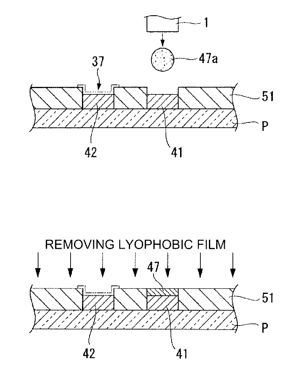
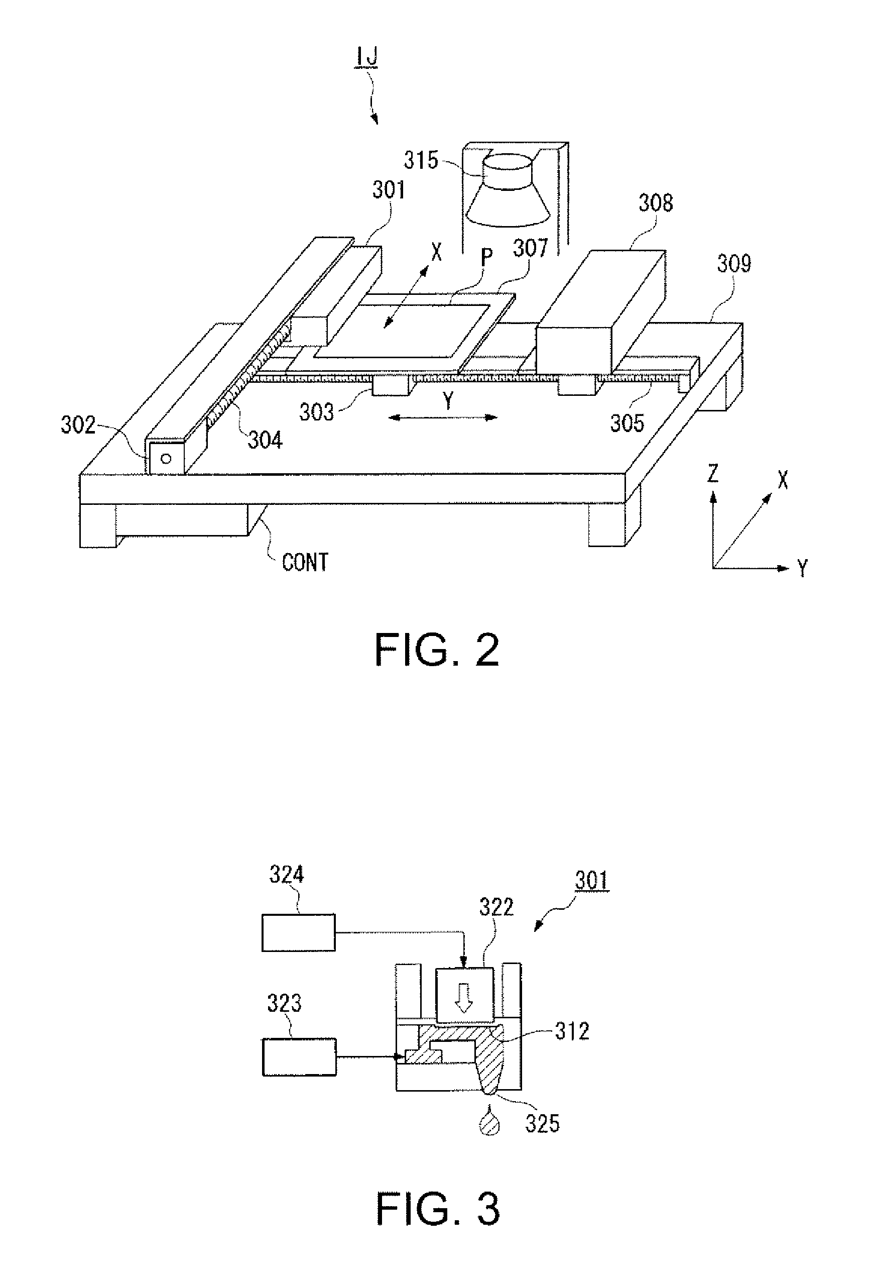
[0050]A method of forming a film pattern, an active matrix substrate, an electro-optic device, and an electronic apparatus according to embodiments of the invention will hereinafter be explained with reference to the accompanying drawings. Note here that, in each of the drawings, contraction scales of layers and parts may be different so as to have recognizable sizes on each of the drawings.

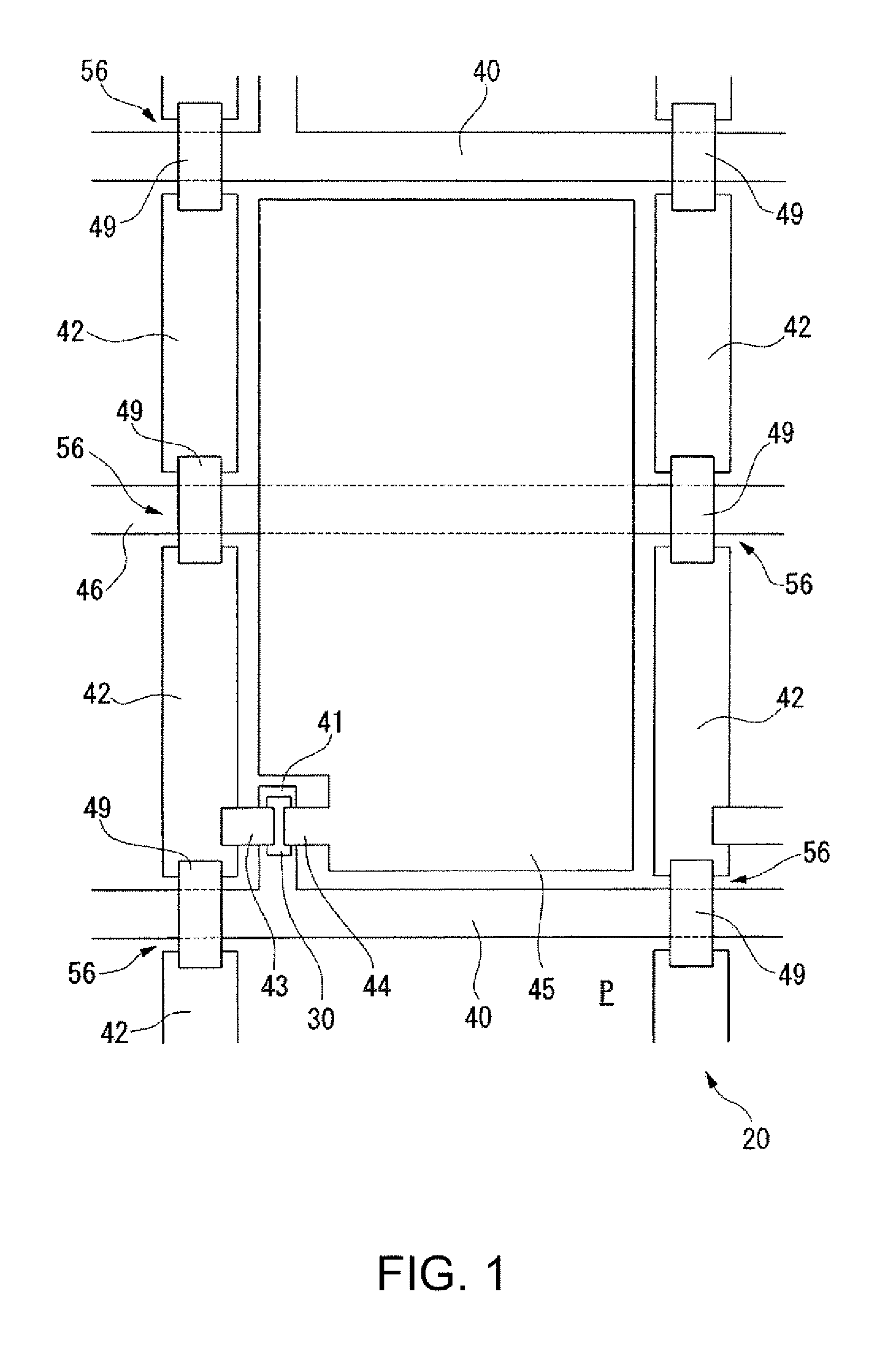
[0051]FIG. 1 is an enlarged plan view showing a schematic configuration of a part of an active matrix substrate 20 provided with a gate wiring (a first film pattern) 40, a source wiring (a second film pattern) 42, and a capacitance lines (the first film pattern) 46.

[0052]The active matrix substrate 20 is provided with a plurality of gate wiring patterns 40 and a plurality of source wiring patterns 42 arranged on a substrate P in a lattice manner. And, the capacitance lines 46 are formed on the substrate P substantially in parallel to the gate wiring pattern 40. Note that the gate wiring 40, the s...


PUM

PropertyMeasurementUnit
weightaaaaaaaaaa
diameteraaaaaaaaaa
diameteraaaaaaaaaa

Abstract

A method of forming a film pattern includes the steps of forming a bank for partitioning a pattern forming area including a first pattern forming area and a second pattern forming area having an intersection with the first pattern forming area and divided in the intersection into sub-areas, disposing a functional liquid to the first pattern forming area to form a first film pattern, and disposing a functional liquid to the sub-areas to form second film patterns, executing a lyophobic process on the entire surface of a substrate including the first film pattern, the second film patterns, and the bank, weakening the lyophobicity on the substrate while selectively maintaining the lyophobicity on predetermined positions of the respective second film patterns formed in a divided condition after executing the lyophobic process, stacking a cap layer on the first film pattern and the second film patterns after weakening the lyophobicity, removing the lyophobicity in the predetermined positions of the respective second film patterns formed in the divided condition after stacking the cap layer, and forming a conductive film between the predetermined position of one of the second film patterns and the predetermined position of another of the second film patterns to electrically connect the second film patterns formed in the divided condition.

Description

BACKGROUND OF THE INVENTION[0001]1. Technical Field[0002]The present invention relates to a method of forming a film pattern, an active matrix substrate, an electro-optic device, and an electronic apparatus.[0003]2. Related Art[0004]A semiconductor device composed of a circuit wiring formed of a conductor thin film (film pattern) disposed therein, a thin film such as an insulating film covering the circuit wiring, and a thin film made of semiconductor all stacked on a substrate has been known from the past. As an efficient method of forming a thin film in such a semiconductor device, a droplet ejection method (inkjet method), in which droplets of a functional liquid containing a thin film material or the like as dispersoid is ejected from a droplet ejection head, and the landed functional liquid is dried to remove the dispersion medium thereby forming the thin film, is known to the public (see, for example, JP-A-11-274671).[0005]In forming a film pattern by the droplet ejection meth...

Claims


Application Information

Patent Timeline
13 May 2008
Publication
US7371698B2
IPC
H01L21/469; G02F1/1345; G09F9/00; G09F9/30; H01L21/3205; H01L21/336; H01L21/768; H01L27/32; H01L29/786
CPC
H01L51/0005; H01L27/3295; H10K71/135; H10K59/122; H05B33/10
Inventors
MORIYA, KATSUYUKI; HIRAI, TOSHIMITSU