
Parallel digital-to-analog-converter

a digital-to-analog converter and parallel technology, applied in the field of digital-to-analog converters, can solve the problems of high power consumption of adc, high system complexity, and inability to use a single adc directly digitizing at the rate fsub>s ,

Active Publication Date: 2008-05-13
NAT SEMICON CORP
View PDF5 Cites 41 Cited by
  • Summary
  • Abstract
  • Description
  • Claims
  • Application Information

AI Technical Summary

Problems solved by technology

It is often prohibitive to use a single ADC directly digitizing at rate fs due to technology limits.
Even when digitizing at a high rate is possible, such an ADC may have large power consumption because, for a given resolution and sample rate, the time-interleaved implementation has the potential to require overall less power than the traditional single ADC implementation.
The main drawback of a parallel time-interleaved analog-to-digital converter is the higher complexity of the system, which, in turn, may result in an overall larger device area compared to the case of a traditional single, higher sampling rate, ADC.
However, the core analog circuits forming the sub-ADCs are unavoidably affected by manufacturing mismatches.
Mismatches between the sub-ADCs introduce severe performance limitations on the practical effectiveness of parallel time-interleaved ADCs.
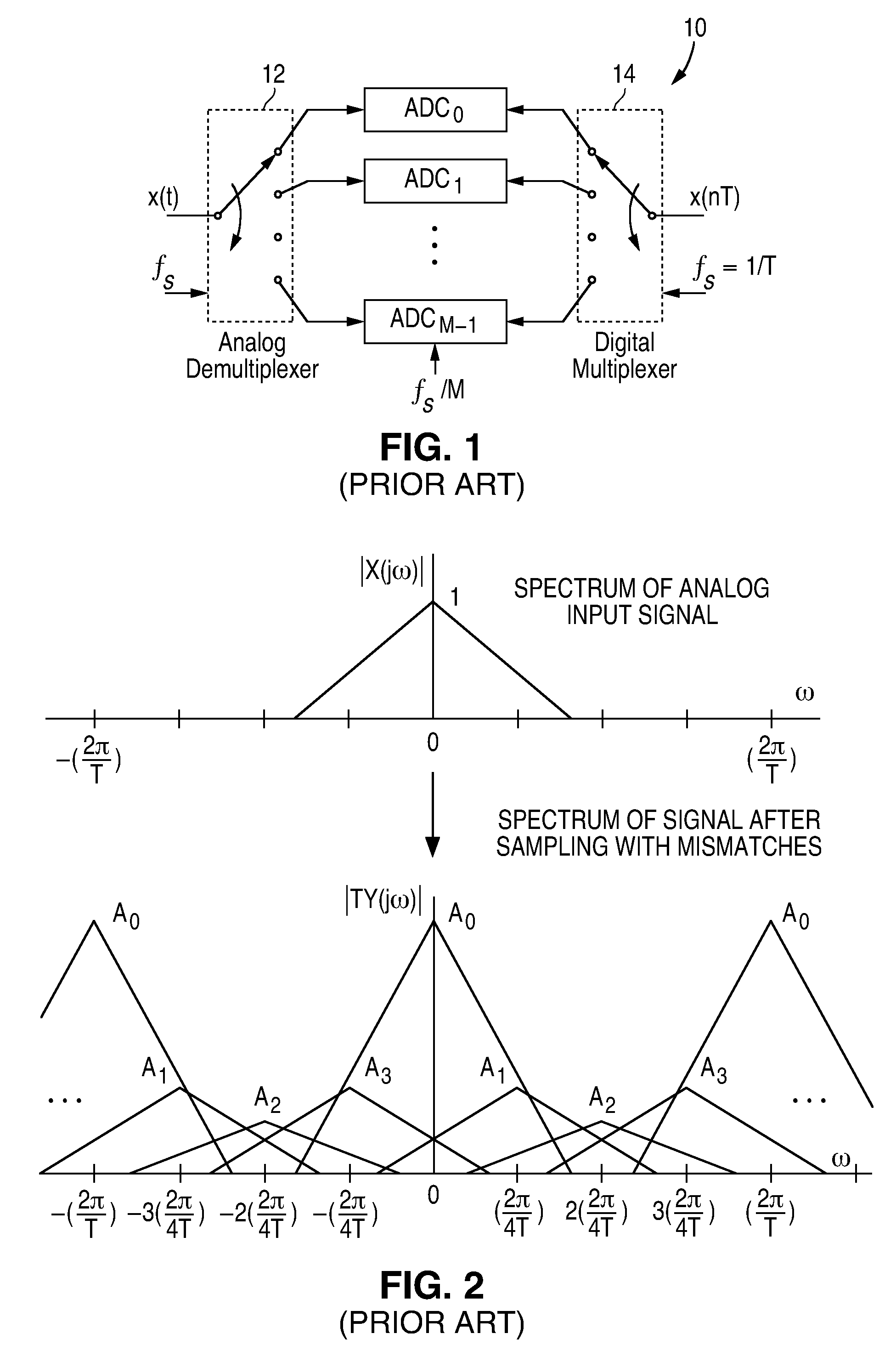
More specifically, gain mismatches, offset mismatches, and sampling clock (timing) skew mismatches between the sub-ADCs result in the introduction of unwanted spurious harmonics in the digitized and demultiplexed output x(nT).
It is well-known that mixing a periodic function with a signal results in spurious images of the original signal at periodic / regular frequency intervals directly related to the periodicity of the modulating function.

Method used


Image

  • Parallel digital-to-analog-converter
  • Parallel digital-to-analog-converter
  • Parallel digital-to-analog-converter

Examples


Embodiment Construction

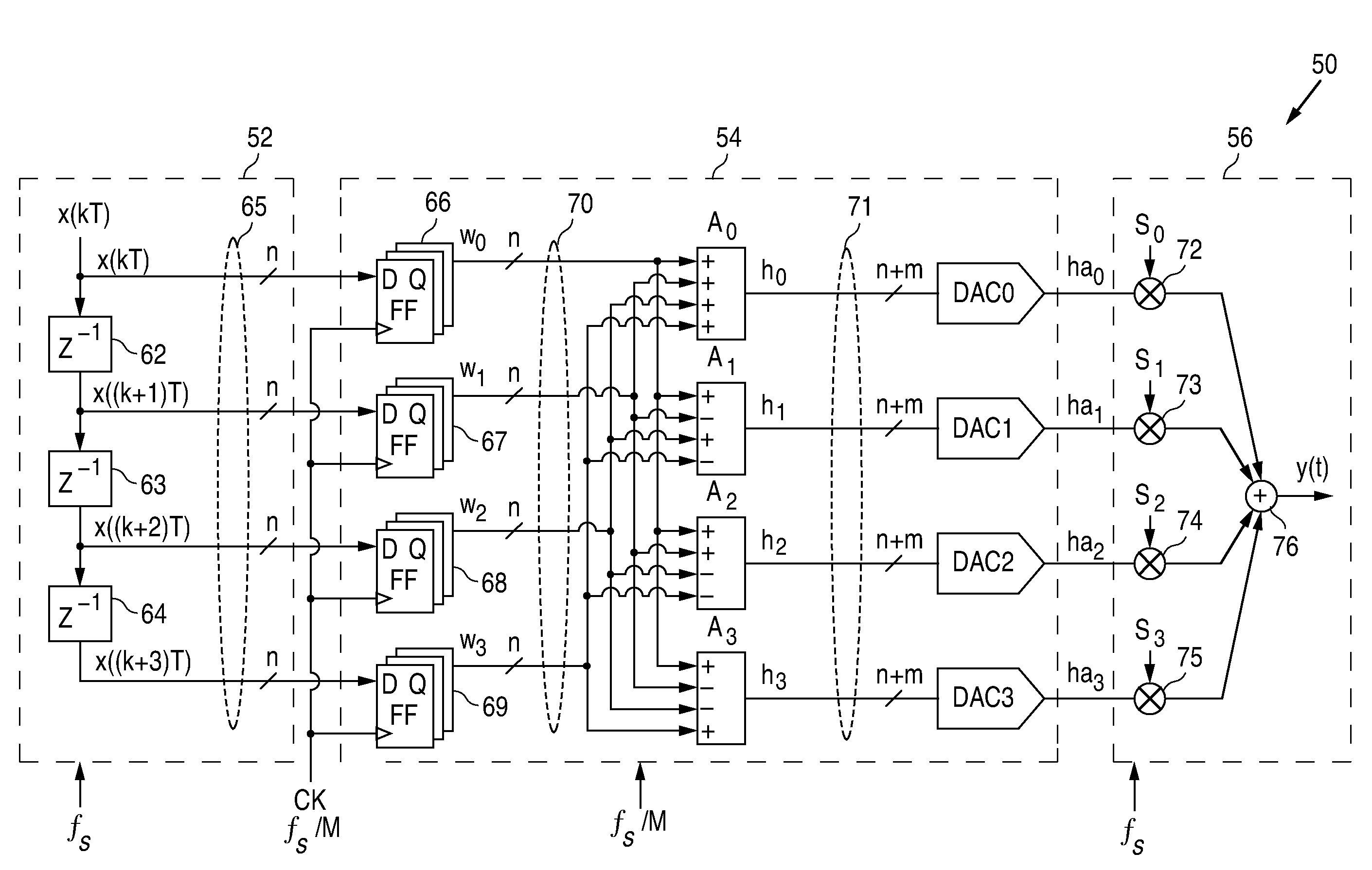
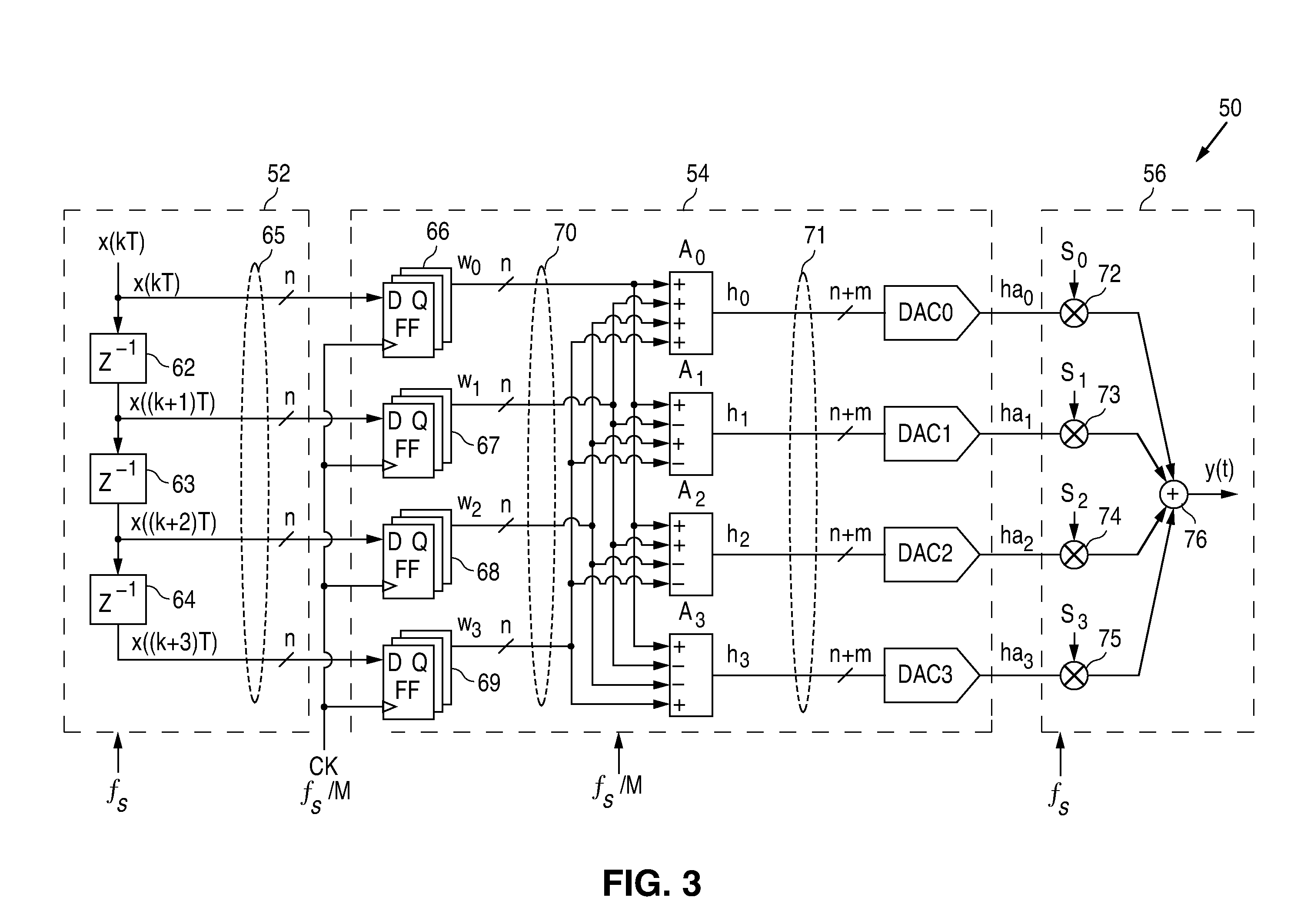
[0019]In accordance with the principles of the present invention, a parallel digital-to-analog converter (DAC) system uses an array of digital-to-analog converters (DACs) to performing parallel digital-to-analog conversion in a time-interleaved manner. The parallel DAC system includes input signal processing operations prior to the conversion operation to minimize errors and unwanted signal effects due to mismatches between the array of DACs. By using a parallel array of DACs, each DAC can operate at a slow rate of speed while the overall DAC system is still capable of providing fast conversion results. As thus configured, the parallel DAC system of the present invention is capable of fast conversion speed, accurate conversion result and low power consumption.

[0020]More specifically, in the parallel DAC system of the present invention, the digital input data stream is sampled at clock rate fs in a time-interleaved manner into an array of M data streams at a clock rate of fs / M. The M...


PUM


Abstract

A method for performing parallel digital-to-analog conversion of an n-bit digital input data signal at a frequency of fs including receiving the n-bit digital input data signal; generating M−1 delayed input data signals, M being the number of parallel conversions channels, the M−1 delayed input data signals having respective increasing amount of unit delay, the digital input data signal and the M−1 delayed input data signals forming M digital signals; holding the M digital signals for a first time period; performing a data transformation of the M digital signals using an M×M Hadamard matrix; generating M (n+m)-bit transformed digital data signals; converting each of the M transformed digital data signals to M analog signals; and performing a reverse data transformation of the M analog signals based on the M×M Hadamard matrix to generate an output analog signal indicative of the n-bit digital input data signal.

Description

FIELD OF THE INVENTION[0001]The invention relates to digital-to-analog converters and, in particular, to a parallel digital-to-analog converter implementing time-interleaving for improved speed and reduced noise and power consumption.DESCRIPTION OF THE RELATED ART[0002]Time-interleaving is a technique that has been applied to analog-to-digital converters to implement parallel analog-to-digital conversion. FIG. 1 is a schematic diagram of a conventional analog-to-digital converter (ADC) implementing time-interleaving. Referring to FIG. 1, an n-bit analog-to-digital converter (ADC) 10 with a sample frequency fs=1 / T, is implemented using an array of M identical n-bit ADCs (ADC0 to ADCM−1), each ADC sampling at frequency fs / M and clocked with appropriately time-delayed sampling control signals. ADC 10 also includes an analog demultiplexer 12 to sample the input analog signal x(t) and a digital multiplexer 14 to generate the digitized output signal x(nT). Analog-to-digital converters ADC...

Claims


Application Information

Patent Timeline
IPC IPC(8): H03M1/66
CPCH03M1/0626H03M1/0836H03M1/1215H03M1/661
Inventor MALOBERTI, FRANCOMANGANARO, GABRIELE
Owner NAT SEMICON CORP
Learn More