Printed circuit board, radio wave receiving converter, and antenna device

a technology of radio wave receiving converter and printed circuit board, which is applied in the direction of printed element electric connection formation, high frequency circuit adaptation, waveguide, etc., can solve the problems of serious quality problems, affecting the performance and quality of the circuit board, and falling off or misalignment of components, so as to prevent the degradation of the performance of a product, reduce the bowing of the printed circuit board, and restrict the effect of loss

Inactive Publication Date: 2008-05-27
SHARP KK
View PDF35 Cites 10 Cited by
  • Summary
  • Abstract
  • Description
  • Claims
  • Application Information

AI Technical Summary

Benefits of technology

[0011]Based on the foregoing, an object of the present invention is to lessen bowing of a printed circuit board after heat treatment by adjusting a conductive pattern formed on a substrate, while preventing degradation in performance of a product and restricting a loss due to an additional step.
[0012]Another object of the present invention is to provide highly reliable, high-performance radio wave receiving converter and antenna device by incorporating the printed circuit board thereto.

Problems solved by technology

On the contrary, a substrate formed of polytetrafluoroethylene and a soft substrate such as a so-called flexible substrate suffer considerable bowing, which greatly affects performance and quality of the circuit board.
Such countermeasures, however, cannot prevent bowing of the circuit board completely, causing falling off or misalignment of component(s) during reflow.
Further, chip crack would occur when mounting the circuit board in an enclosure, possibly causing a serious problem regarding quality.
Still further, the additional steps of massaging the substrate and others would lead to a considerable loss.

Method used


Image

  • Printed circuit board, radio wave receiving converter, and antenna device
  • Printed circuit board, radio wave receiving converter, and antenna device
  • Printed circuit board, radio wave receiving converter, and antenna device

Examples


first embodiment

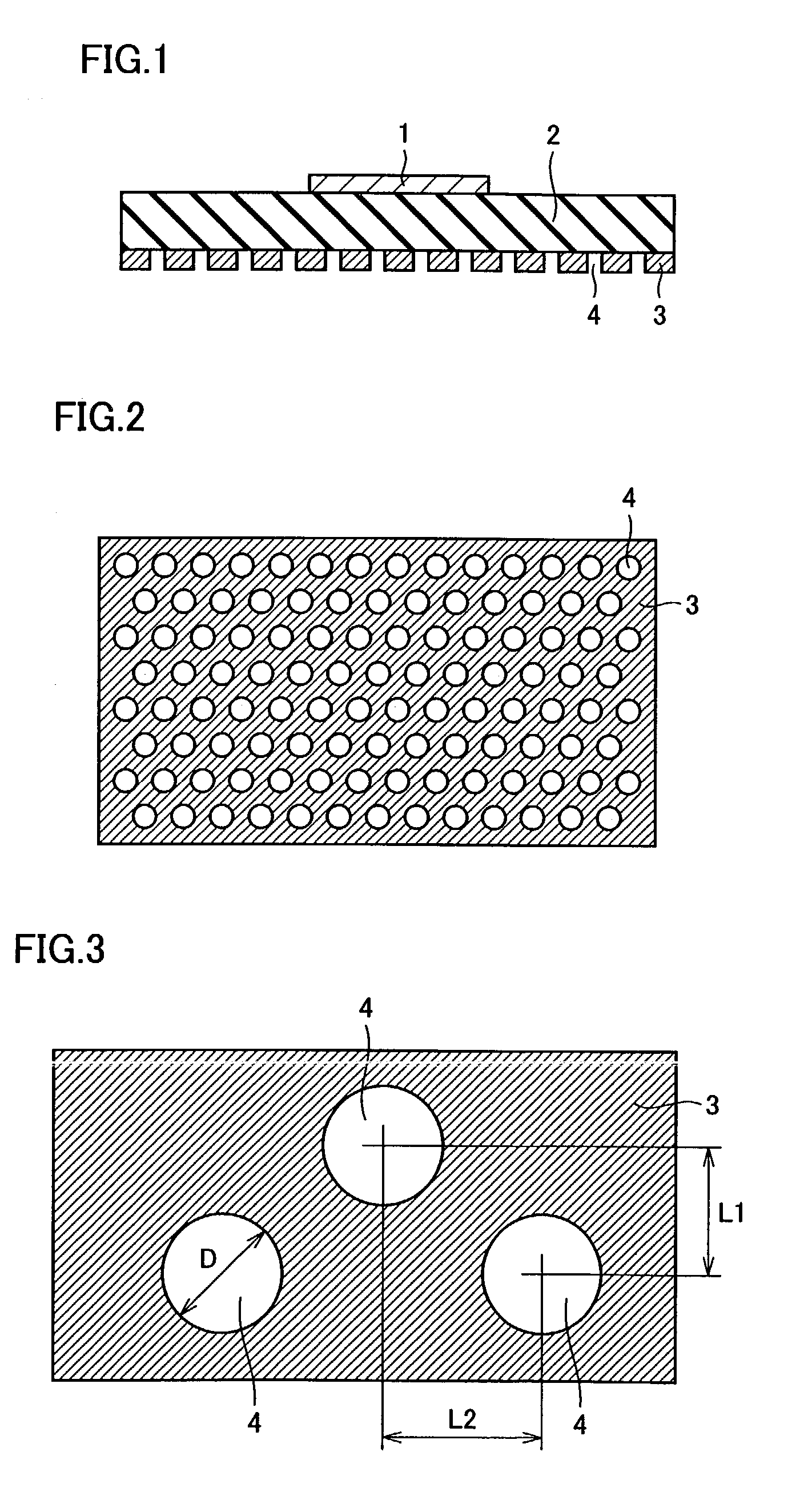
[0047]FIG. 1 schematically shows the microstrip line portion of the printed circuit board according to the first embodiment. FIG. 2 shows the rear surface of the printed circuit board shown in FIG. 1.

[0048]As shown in FIGS. 1 and 2, the printed circuit board includes a substrate (base material) 2 of a dielectric material (insulator), a strip line (first conductive pattern) 1 as a transmission line formed on a front surface of substrate 2, and a ground metal layer (ground pattern) 3 formed to cover an entire rear surface of substrate 2.

[0049]Substrate 2 is formed of glass fiber and polytetrafluoroethylene, for example. Strip line 1 and ground metal layer 3 are formed, e.g., of copper. The copper surfaces may be coated with gold plating, solder plating, organic resin or the like to prevent corrosion.

[0050]A plurality of openings 4 are provided in ground metal layer 3. In the example shown in FIGS. 1 and 2, openings 4 are formed over the entire rear surface of substrate 2 at approximat...

second embodiment

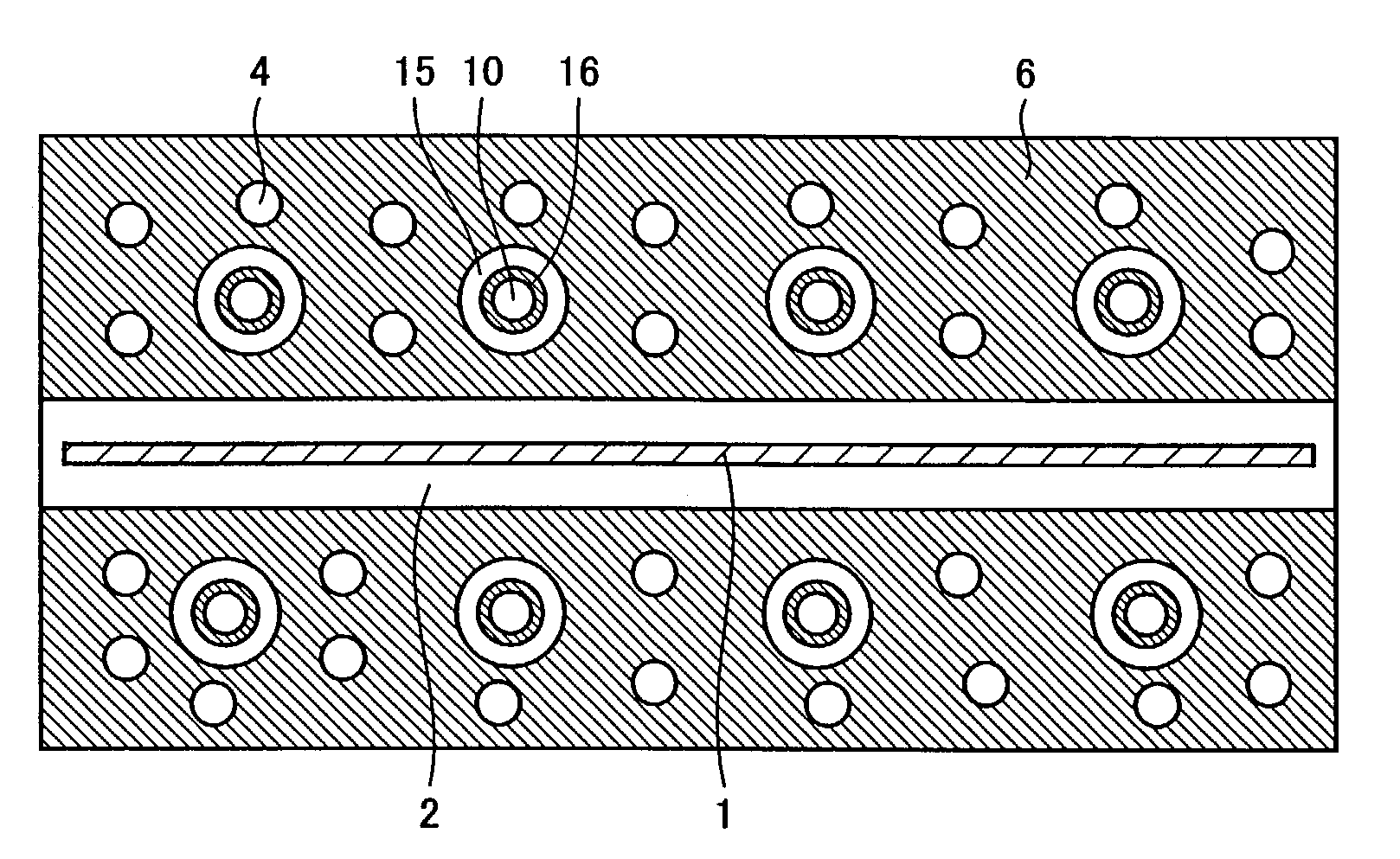
[0066]The second embodiment of the present invention is explained with reference to FIG. 4. FIG. 4 is a partial top plan view of the printed circuit board of the second embodiment.

[0067]As shown in FIG. 4, a ground pattern 6 may be provided on a microstrip line surface of substrate 2 on which a strip line 1 is formed, and openings 4 may be provided in the relevant ground pattern 6. In this case, again, the residual copper ratio can be adjusted, and thus, the bowing of the circuit board can be reduced. The shape and designing method of opening 4 are as in the first embodiment.

third embodiment

[0068]The third embodiment of the present invention is explained with reference to FIG. 7. FIG. 7 is a partial cross sectional view of the printed circuit board of the third embodiment. In the third embodiment, the present invention is applied to a printed circuit board having laminated substrates.

[0069]As shown in FIG. 7, the printed circuit board has substrates 7, 9 formed of different materials, an intermediate layer 8 formed between substrates 7 and 9, and strip lines (transmission lines) 1 formed on surfaces of respective substrates 7, 9.

[0070]Substrate 7 is formed, e.g., of FR-4, and substrate 9 is formed, e.g., of polytetrafluoroethylene. Intermediate layer 8 is formed of a metal layer such as copper.

[0071]In the third embodiment, via holes 5 reaching respective substrates 7, 9 are formed in intermediate layer 8. Provision of such via holes 5 restricts occurrence of internal stress due to the difference in thermal expansion coefficient of the different materials during the he...


PUM


Abstract

A printed circuit board has a substrate formed of an insulator, a strip line provided on a front surface of the substrate, and a ground metal layer provided on a rear surface of the substrate. An opening is provided in the ground metal layer to reach the substrate. A radio wave receiving converter and an antenna device each include the printed circuit board.

Description

BACKGROUND OF THE INVENTION[0001]1. Field of the Invention[0002]The present invention relates to printed circuit boards, radio wave receiving converters and antenna devices. More particularly, the present invention relates to a structure of printed circuit board suffering less bowing after heat treatment for reflow or the like, and a radio wave receiving converter and an antenna device each provided with the relevant printed circuit board.[0003]2. Description of the Background Art[0004]Conventionally, a printed circuit board having a wiring pattern formed on a substrate comprised of an insulator is widely known. An example of such a printed circuit board is a high-frequency circuit board. A microstrip line and a coplanar line are often used as lines formed on the high-frequency circuit board.[0005]A substrate portion on which, e.g., a microstrip line is formed (hereinafter, referred to as the “microstrip substrate”) consists of a component surface (the surface on which a transmissio...

Claims


Application Information

Patent Timeline
Patent Type & Authority Patents(United States)
IPC IPC(8): H01R12/04H05K1/11H01P3/02H01Q1/24H01Q1/38H05K1/02H05K3/42
CPCH01Q1/247H01Q1/38H05K1/0201H05K1/0224H05K1/0271H05K3/4688H05K1/0253H05K2201/09718H05K3/42H05K2201/062H05K2201/0715H05K2201/093H05K2201/09681H05K1/116
Inventor SOMEI, JUNICHI
Owner SHARP KK
Why Eureka
Try Eureka