Rapid conductive cooling using a secondary process plane

a secondary process plane and process plane technology, applied in semiconductor/solid-state device testing/measurement, furnaces, muffle furnaces, etc., can solve the problems of substrate plastic deformation or warpage, integrated circuits have evolved into complex devices, and implanted films may develop a high level of internal stress

Active Publication Date: 2008-05-27
APPLIED MATERIALS INC
View PDF18 Cites 239 Cited by
  • Summary
  • Abstract
  • Description
  • Claims
  • Application Information

AI Technical Summary

Benefits of technology

[0013]In another embodiment, a method for thermally treating a substrate is described. The method includes providing a substrate to a chamber at a first temperature, heating the substrate in a first time period to a second temperature, heating the substrate to third temperature in a second time period, cooling the substrate to the second temperature in the second time period, and cooling the substrate to the first temperature in a third time period, wherein the second time period is less than about 2 seconds.

Problems solved by technology

Integrated circuits have evolved into complex devices that can include millions of transistors, capacitors, and resistors on a single chip.
During ion implantation, the implanted film may develop a high level of internal stress.
However, as processing parameters continue to evolve, temperature ramp up and heating uniformity during RTP requires closer monitoring and control.
While conventional RTP chambers rely on the radiant heat source to rapidly heat the substrate to a desired temperature, the challenges arise when the substrate requires cooling to improve heating uniformity, and / or when the substrate needs to be rapidly cooled.
For example, if a significant temperature gradient exists across the substrate, the substrate may plastically deform or warp, which may be detrimental to subsequent processes performed on the substrate.

Method used


Image

  • Rapid conductive cooling using a secondary process plane
  • Rapid conductive cooling using a secondary process plane
  • Rapid conductive cooling using a secondary process plane

Examples


Embodiment Construction

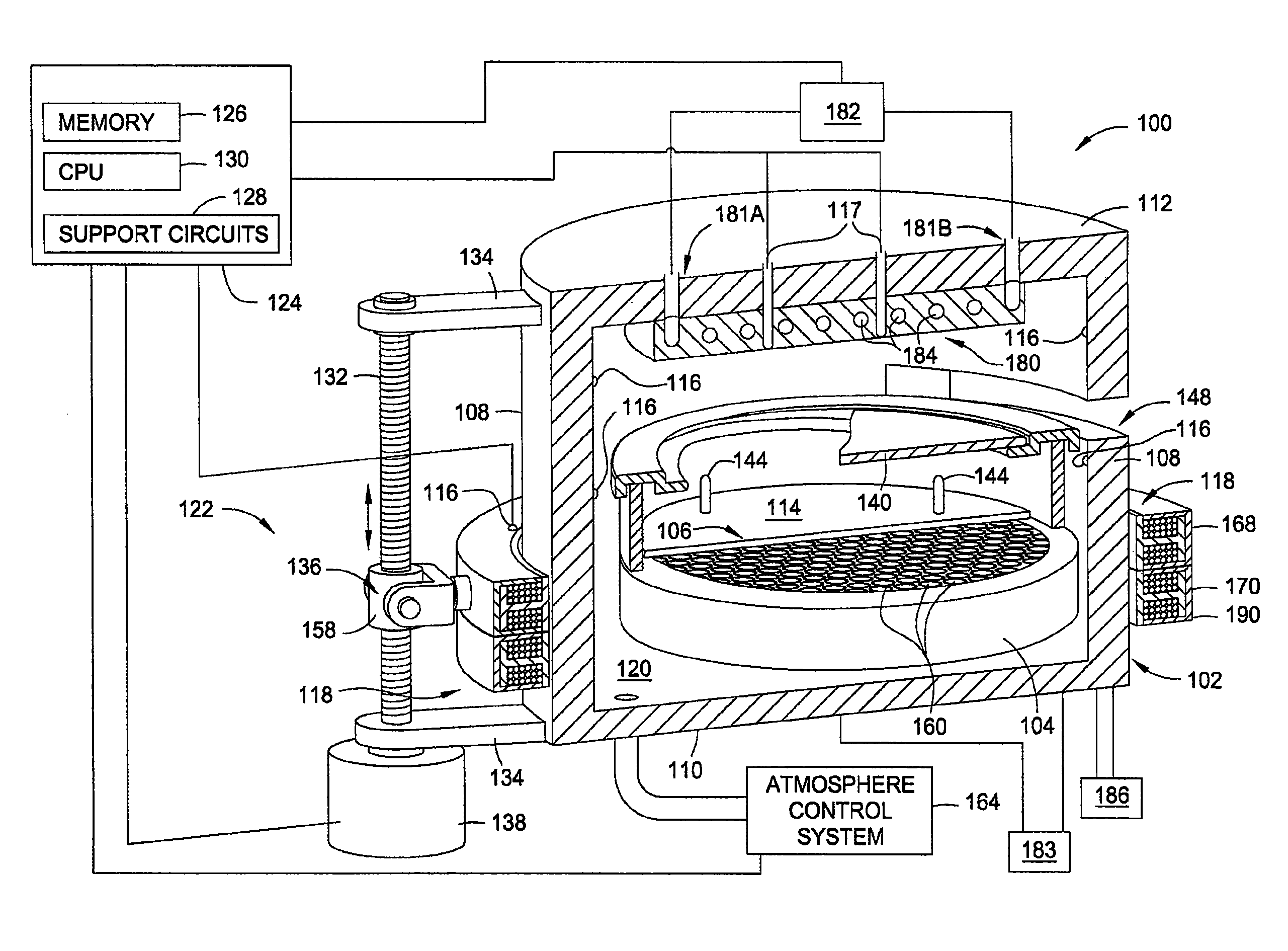
[0020]FIG. 1 is a simplified isometric view of one embodiment of a rapid thermal processing chamber 100. Examples of rapid thermal processing chambers that may be adapted to benefit from the invention are Quantum X plus and CENTURA® thermal processing systems, both available from Applied Materials, Inc., located in Santa Clara, Calif. Although the apparatus is described as utilized within a rapid thermal processing chamber, embodiments described herein may be utilized in other processing systems and devices where at least two temperature zones within one processing region is desired, such as substrate support platforms adapted for robot handoffs, orientation devices, deposition chambers, etch chambers, electrochemical processing apparatuses and chemical mechanical polishing devices, among others, particularly where the minimization of particulate generation is desired.

[0021]The processing chamber 100 includes a contactless or magnetically levitated substrate support 104, a chamber b...


PUM

PropertyMeasurementUnit
emissivityaaaaaaaaaa
temperatureaaaaaaaaaa
emissivityaaaaaaaaaa

Abstract

A method and apparatus for thermally processing a substrate is described. The apparatus includes a substrate support configured to move linearly and/or rotationally by a magnetic drive. The substrate support is also configured to receive a radiant heat source to provide heating region in a portion of the chamber. An active cooling region comprising a cooling plate is disposed opposite the heating region. The substrate may move between the two regions to facilitate rapidly controlled heating and cooling of the substrate.

Description

BACKGROUND OF THE INVENTION[0001]1. Field of the Invention[0002]Embodiments of the present invention generally relate to a method and apparatus for processing semiconductor substrates. More specifically, to a method and apparatus for thermally treating semiconductor substrates.[0003]2. Description of the Related Art[0004]Integrated circuits have evolved into complex devices that can include millions of transistors, capacitors, and resistors on a single chip. The evolution of chip design continually requires faster circuitry and greater circuit density that demand increasingly precise fabrication processes. One fabrication process frequently used is ion implantation.[0005]Ion implantation is particularly important in forming transistor structures on semiconductor substrates and may be repeated many times during chip fabrication. During ion implantation, a semiconductor substrate, typically comprising a silicon material and / or a silicon containing film, is bombarded by a beam of elect...

Claims


Application Information

Patent Timeline
Patent Type & Authority Patents(United States)
IPC IPC(8): F27D11/00F26B19/00
CPCC30B31/14H01L21/67098H01L21/67109H01L21/67115H01L22/10H01L21/30H01L2924/0002H01L2924/00H01L21/324
Inventor SORABJI, KHURSHEDLERNER, ALEXANDER N.
Owner APPLIED MATERIALS INC
Why Eureka
Try Eureka