
Pendeoepitaxial gallium nitride semiconductor layers on silicon carbide substrates

a gallium nitride and silicon carbide substrate technology, applied in the direction of semiconductor lasers, crystal growth processes, polycrystalline material growth, etc., can solve the problems of low defect density of gallium nitride semiconductor layers, undesired ridge growth or lateral overgrowth, etc., and achieve high-performance microelectronic devices. , the effect of low defect density

Inactive Publication Date: 2008-05-27
NORTH CAROLINA STATE UNIV
View PDF62 Cites 5 Cited by
  • Summary
  • Abstract
  • Description
  • Claims
  • Application Information

AI Technical Summary

Benefits of technology

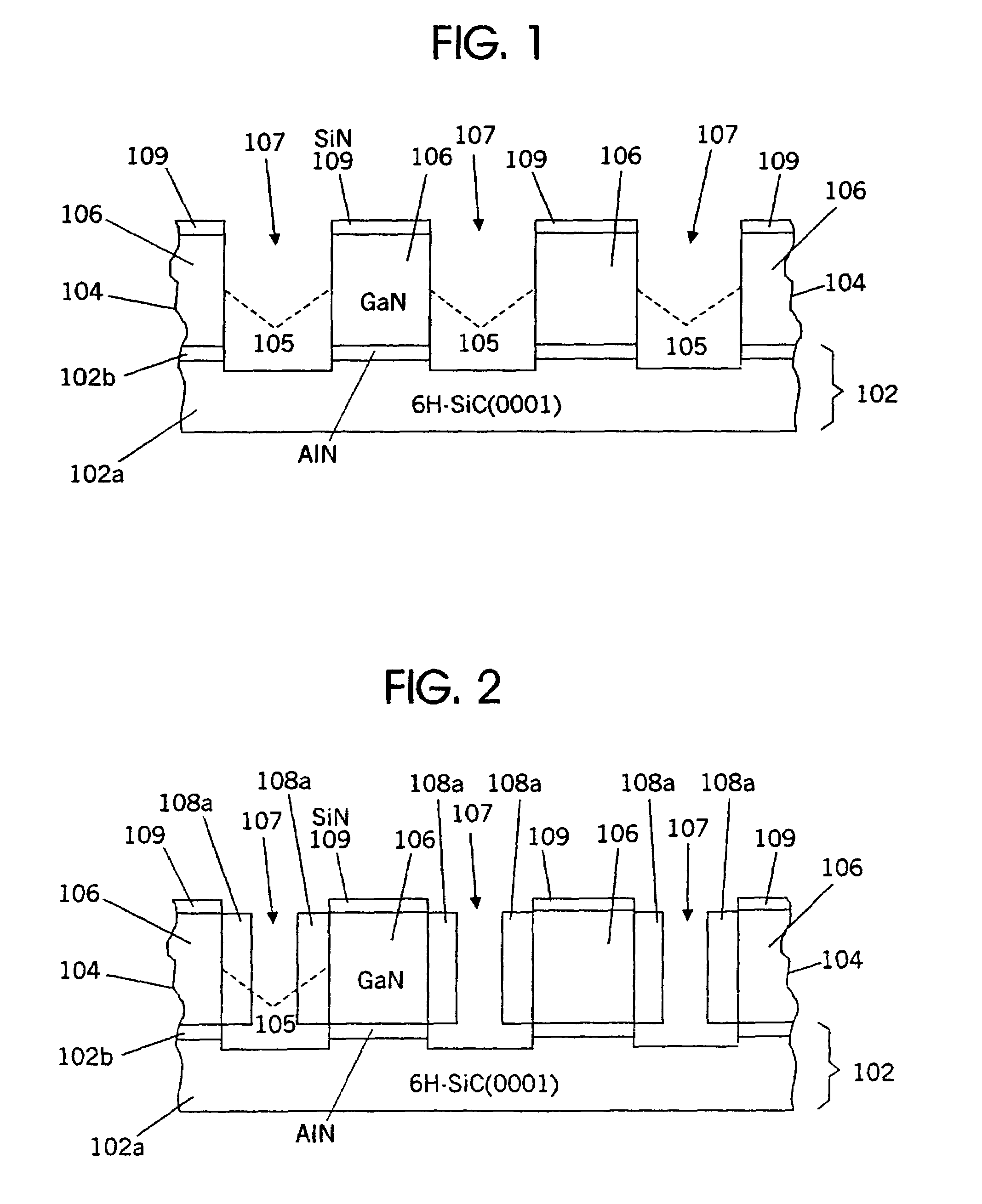
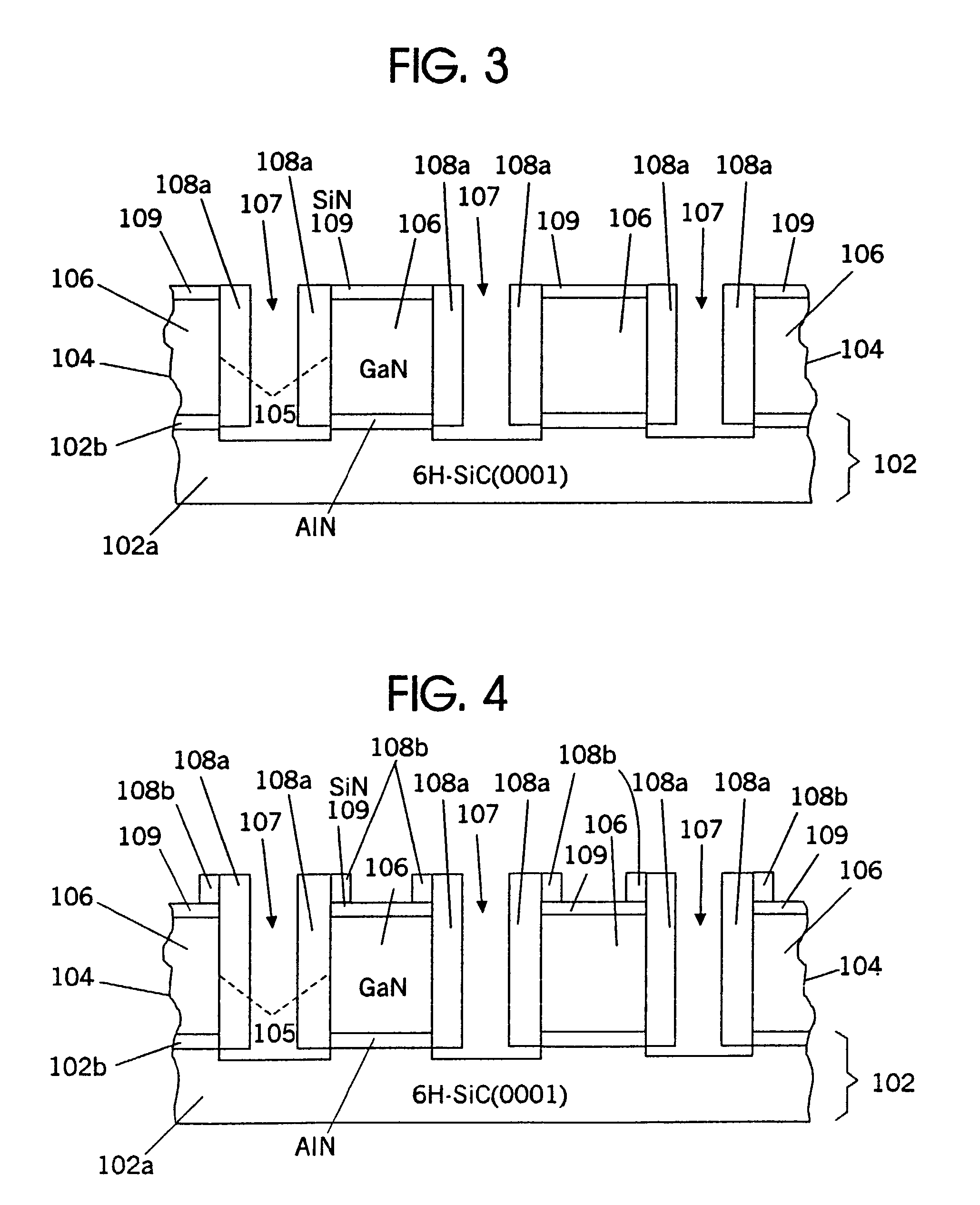
The present invention provides improved methods of fabricating gallium nitride semiconductor layers with low defect densities. These methods involve masking an underlying gallium nitride layer with a mask that includes openings and etching the layer through the openings to form a plurality of posts and trenches. The lateral growth of the gallium nitride layer from the sidewalls of the posts is then continued until the layers coalesce on the mask, resulting in a continuous layer of relatively defect-free gallium nitride. The invention also provides a mask that acts as a capping layer to force the selective homoepitaxial growth of gallium nitride on the sidewalls of the posts, while preventing nucleation and vertical growth on the top of the posts. The use of this mask results in a high-quality, low-defect density gallium nitride semiconductor layer.

Problems solved by technology

A major problem in fabricating gallium nitride-based microelectronic devices is the fabrication of gallium nitride semiconductor layers having low defect densities.
As disclosed in these publications, undesired ridge growth or lateral overgrowth may occur under certain conditions.

Method used


Image

  • Pendeoepitaxial gallium nitride semiconductor layers on silicon carbide substrates
  • Pendeoepitaxial gallium nitride semiconductor layers on silicon carbide substrates
  • Pendeoepitaxial gallium nitride semiconductor layers on silicon carbide substrates

Examples


Embodiment Construction

[0021]The present invention now will be described more fully hereinafter with reference to the accompanying drawings, in which preferred embodiments of the invention are shown. This invention may, however, be embodied in many different forms and should not be construed as limited to the embodiments set forth herein; rather, these embodiments are provided so that this disclosure will be thorough and complete, and will fully convey the scope of the invention to those skilled in the art. In the drawings, the thickness of layers and regions are exaggerated for clarity. Like numbers refer to like elements throughout. It will be understood that when an element such as a layer, region or substrate is referred to as being “on” or “onto” another element, it can be directly on the other element or intervening elements may also be present. Moreover, each embodiment described and illustrated herein includes its complementary conductivity type embodiment as well.

[0022]Referring now to FIGS. 1-6,...


PUM

PropertyMeasurementUnit
temperatureaaaaaaaaaa
thickaaaaaaaaaa
thickaaaaaaaaaa

Abstract

An underlying gallium nitride layer on a silicon carbide substrate is masked with a mask that includes an array of openings therein, and the underlying gallium nitride layer is etched through the array of openings to define posts in the underlying gallium nitride layer and trenches therebetween. The posts each include a sidewall and a top having the mask thereon. The sidewalls of the posts are laterally grown into the trenches to thereby form a gallium nitride semiconductor layer. During this lateral growth, the mask prevents nucleation and vertical growth from the tops of the posts. Accordingly, growth proceeds laterally into the trenches, suspended from the sidewalls of the posts. The sidewalls of the posts may be laterally grown into the trenches until the laterally grown sidewalls coalesce in the trenches to thereby form a gallium nitride semiconductor layer. The lateral growth from the sidewalls of the posts may be continued so that the gallium nitride layer grows vertically through the openings in the mask and laterally overgrows onto the mask on the tops of the posts, to thereby form a gallium nitride semiconductor layer. The lateral overgrowth can be continued until the grown sidewalls coalesce on the mask to thereby form a continuous gallium nitride semiconductor layer. Microelectronic devices may be formed in the continuous gallium nitride semiconductor layer.

Description

CROSS-REFERENCE TO RELATED APPLICATIONS[0001]This application is a continuation of application Ser. No. 09 / 717,717, filed Nov. 21, 2000 (now U.S. Pat. No. 6,462,355), entitled Pendeoepitaxial Methods of Fabricating Gallium Nitride Semiconductor Layers On Silicon Carbide Substrates by Lateral Growth From Sidewalls of Masked Posts, and Gallium Nitride Semiconductor Structures Fabricated Thereby, which itself is a continuation of application Ser. No. 09 / 198,784, filed Nov. 24, 1998 (now U.S. Pat. No. 6,177,688), entitled Pendeoepitaxial Gallium Nitride Semiconductor Layers on Silicon Carbide Substrates. Both of these applications are assigned to the assignee of the present application, the disclosures of both of which are hereby incorporated herein by reference in their entirety as if set forth fully herein.FEDERALLY SPONSORED RESEARCH[0002]This invention was made with Government support under Office of Naval Research Contract Nos. N00014-96-1-0765, N00014-98-1-0384, and N00014-98-1-06...

Claims


Application Information

Patent Timeline
Patent Type & Authority Patents(United States)
IPC IPC(8): H01L29/20C30B29/38C30B25/02H01L21/20H01L21/205H01L33/12H01L33/32H01L33/34H01S5/323
CPCC30B25/02C30B29/406H01L21/02378H01L21/02458H01L21/0254H01L21/02639H01L21/0265H01L21/20
Inventor LINTHICUM, KEVIN J.GEHRKE, THOMASTHOMSON, DARREN B.CARLSON, ERIC P.RAJAGOPAL, PRADEEPDAVIS, ROBERT F.
Owner NORTH CAROLINA STATE UNIV
Learn More