High performance sub-system design and assembly

a sub-system and high-performance technology, applied in the direction of sustainable buildings, semiconductor/solid-state device testing/measurement, instruments, etc., can solve the problems of limiting the application of embedded dram, process parameters that enhance the performance of logic or dram, and be compromised, so as to achieve maximum performance and minimum cost

Inactive Publication Date: 2008-05-27
QUALCOMM INC
View PDF12 Cites 16 Cited by
  • Summary
  • Abstract
  • Description
  • Claims
  • Application Information

AI Technical Summary

Benefits of technology

[0024]The first integrated circuit chip could be fabricated using a first type of semiconductor process and the second integrated circuit chip would be fabricated with a second type of semiconductor process that is not compatible with the first type of semiconductor process, and so on. As an example, the first integrated circuit chip could be an array of memory cells and the second integrated circuit chip would contain electronic circuitry formed with a process not compatible with a process of the array of memory cells. Alternatively, the second integrated circuit chip is an array of memory cells and the first integrated circuit chip contains electronic circuitry formed with a process not compatible with a process of the array of memory cells. Other integrated circuit chips could be fabricated in other ways. Fabricating the first integrated circuit chip using its optimum semiconductor process, fabricating the second integrated circuit chip using its optimum semiconductor process, and then joining the first and second integrated circuit chips by this invention creates a multiple chip integrated circuit structure having maximum performance with minimum cost.

Problems solved by technology

The manufacture of embedded Dynamic Random Access Memory (DRAM) requires that process parameters that enhance the performance of the logic or the DRAM, if separately formed on semiconductor chips, be compromised when DRAM is embedded into an array of logic gates on the same semiconductor chip.
This compromise has limited the application of embedded DRAM.
If there is no compromise in the process parameters to enhance the performance of logic or the embedded DRAM, the manufacturing process becomes very complicated and costly.
Moreover, because of the structure of the embedded DRAM and the logic, burn-in of the embedded DRAM is not possible and embedding of DRAM with logic is not a reliable design solution.

Method used


Image

  • High performance sub-system design and assembly
  • High performance sub-system design and assembly
  • High performance sub-system design and assembly

Examples


Embodiment Construction

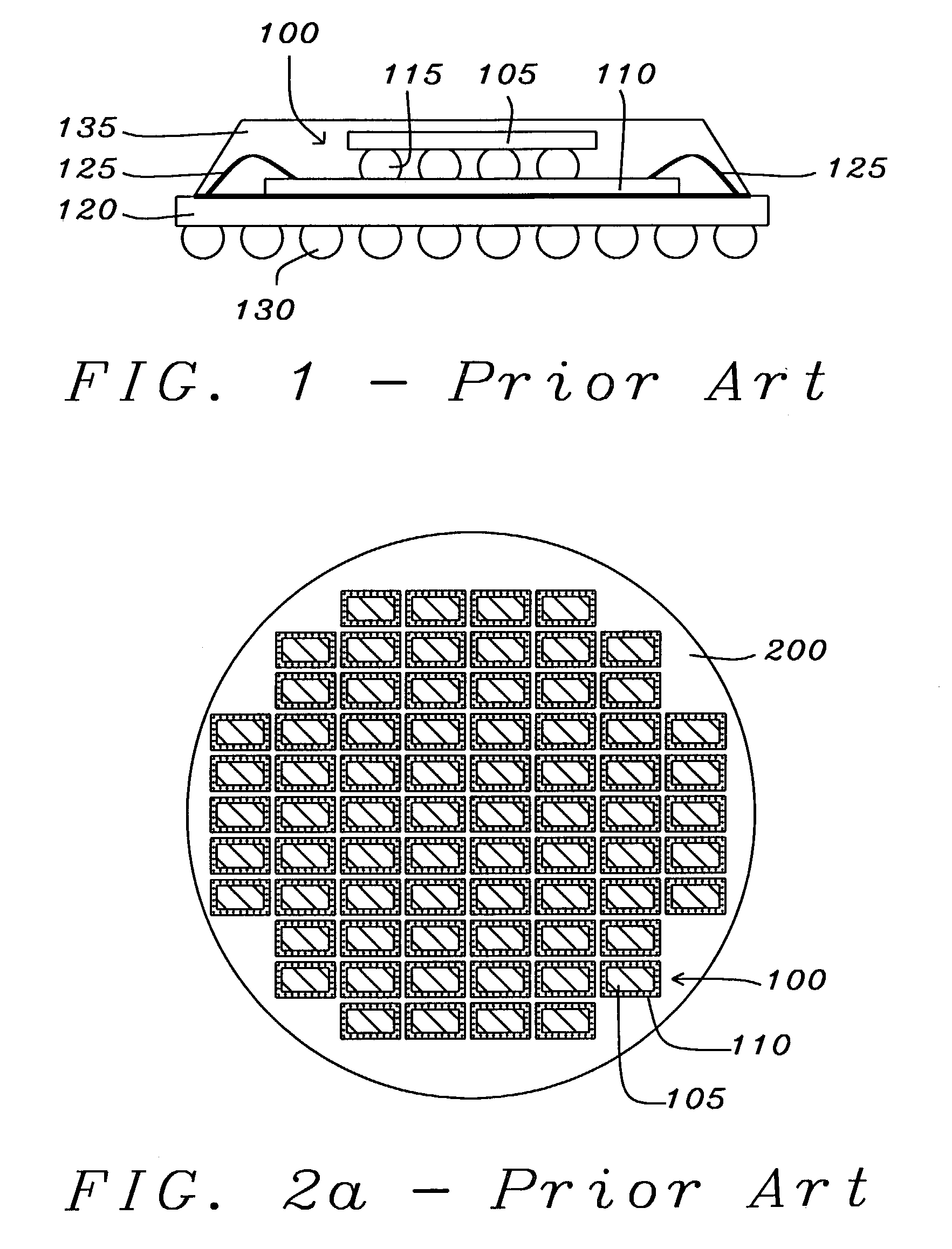
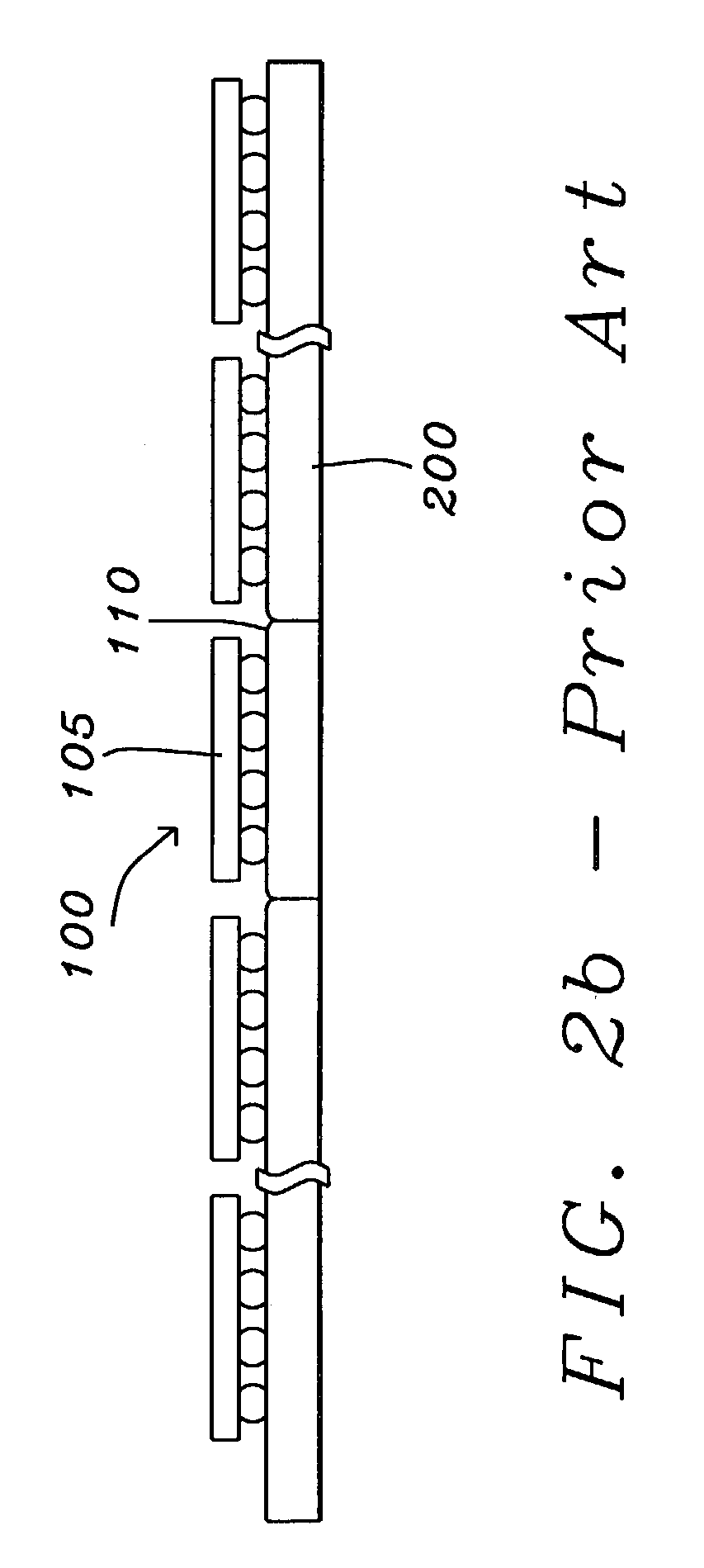
[0033]The process and structure of the present invention can be extended to any kind of format of multi-chip module. For example, two or a few chips 72 and 74 may be mounted on the same side of the ball grid array substrate 76 as shown in FIG. 7a. The ball grid array 76 is shown attached to the substrate 78. The substrate can be laminated printed circuit boards, or ceramic, glass, aluminum, copper, or any kind of substrates. FIG. 7b through 7d illustrate other examples of multiple chip configurations. In all of these examples, more than the two chips shown can be connected together. The following figures illustrate a “chip-on-chip” structure. It will be understood by those skilled in the art that the present invention should not be limited to any of the examples shown, but can be extended and applied to any kind of format of multiple chip module.

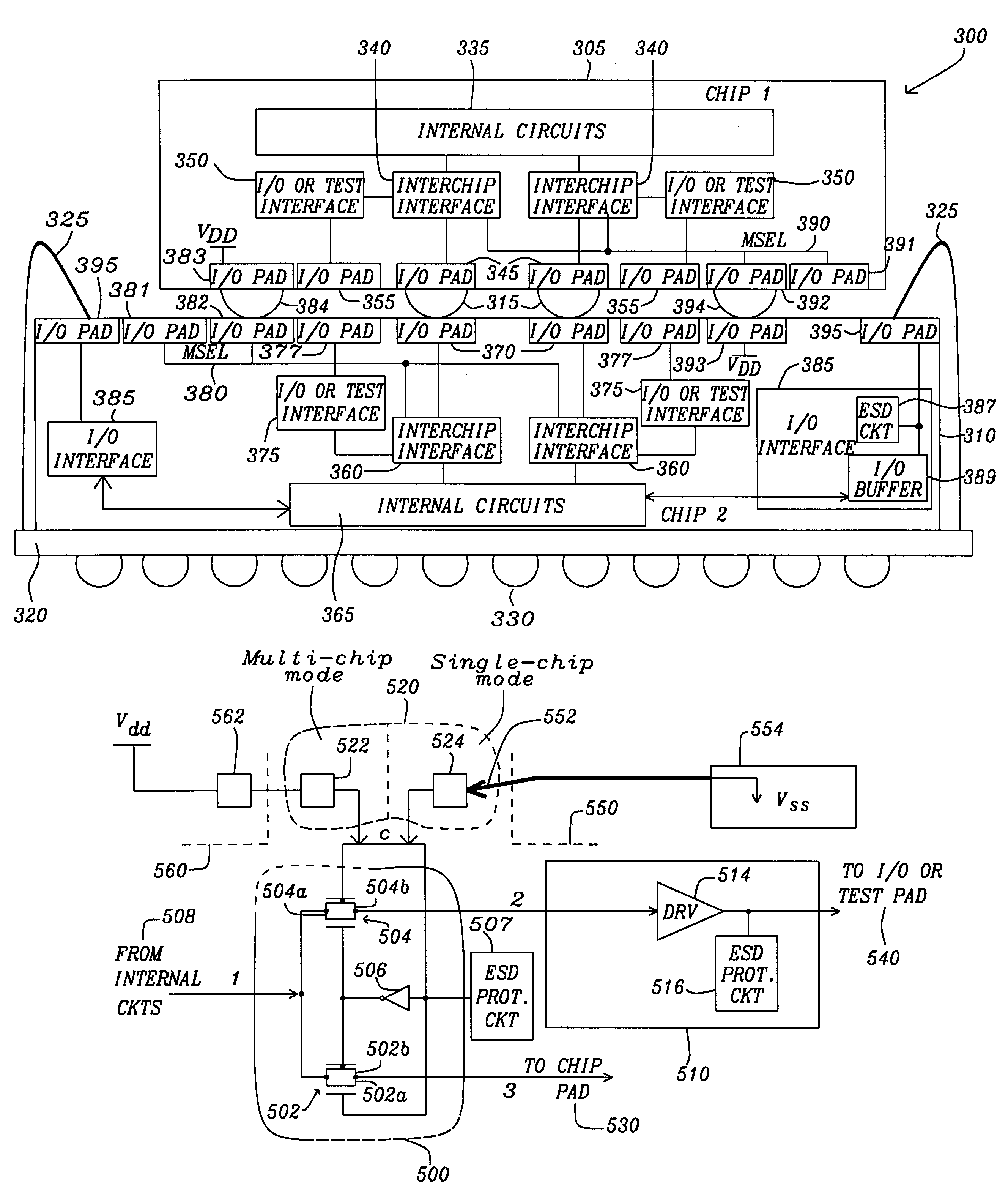
[0034]A “chip-on-chip” structure 300 is shown in FIG. 3. A first integrated circuit chip 305 is attached to a second integrated circuit chi...


PUM


Abstract

A multiple integrated circuit chip structure provides interchip communication between integrated circuit chips of the structure with no ESD protection circuits and no input/output circuitry. The interchip communication is between internal circuits of the integrated circuit chips. The multiple integrated circuit chip structure has an interchip interface circuit to selectively connect internal circuits of the integrated circuits to test interface circuits having ESD protection circuits and input/output circuitry designed to communicate with external test systems during test and burn-in procedures. The multiple interconnected integrated circuit chip structure has a first integrated circuit chip mounted to one or more second integrated circuit chips to physically and electrically connect the integrated circuit chips to one another. The first integrated circuit chips have interchip interface circuits connected each other to selectively communicate between internal circuits of the each other integrated circuit chips or test interface circuits, connected to the internal circuits of each integrated circuit chip to provide stimulus and response to said internal circuits during testing procedures. A mode selector receives a signal external to the chip to determine whether the communication is to be with one of the other connected integrated circuit chips or in single chip mode, such as with the test interface circuits. ESD protection is added to the mode selector circuitry.

Description

[0001]This application is a Division application of Ser. No. 09 / 849,039 filed on May 4, 2001, now issued as U.S. Pat. No. 6,586,266, which a Continuation-in-Part application of 09 / 729,152 filed on Dec. 4, 2000, now issued as U.S. Pat. No. 6,303,996, which is a Division application of Ser. No. 09 / 258,911 filed on Mar. 1, 1999, now issued as U.S. Pat. No. 6,180,426.[0002]This patent application is related to application Ser. No. 09 / 246,303, filed on Feb. 8, 1999, now U.S. Pat. No. 6,356,958.[0003]This invention is related to the application Ser. No. 09 / 961,767, filed on Sep. 21, 2001, now pending.[0004]This invention is related to the application Ser. No. 11 / 181,175, filed on Jul. 14, 2005, now pending.[0005]This patent application is related to application Ser. No. 09 / 422,174, filed on Oct. 22, 1999, now U.S. Pat. No. 6,555,398.[0006]This patent application is related to application Ser. No. 10 / 385,953, filed on Mar. 11, 2003, now pending.BACKGROUND OF THE INVENTION[0007]1. Field of ...

Claims


Application Information

Patent Timeline
Patent Type & Authority Patents(United States)
IPC IPC(8): H01L23/48H01L21/66G01R31/28G01R31/319G06F13/38H01L21/98
CPCG01R31/31905G01R31/31926G06F13/385H01L23/60H01L25/0657H01L25/50G01R31/2884G01R31/2856Y02B60/1235H01L2224/16145H01L2224/48091H01L2224/48227H01L2225/06513H01L2225/06527H01L2225/06596H01L2924/09701H01L2924/15311H01L2924/1532Y02B60/1228H01L2924/10253H01L24/48H01L2924/00014H01L2924/00H01L2224/73207H01L2224/05599H01L2224/45099H01L2224/85399H01L2924/14H01L2924/181Y02D10/00H01L2224/45015H01L2924/207H01L2924/00012
Inventor LIN, MOU-SHIUNG
Owner QUALCOMM INC
Why Eureka
Try Eureka