
Methods for improving the cracking resistance of low-k dielectric materials

Inactive Publication Date: 2008-06-03
NOVELLUS SYSTEMS
View PDF118 Cites 31 Cited by
  • Summary
  • Abstract
  • Description
  • Claims
  • Application Information

AI Technical Summary

Benefits of technology

[0007]To achieve the foregoing, and in accordance with the purpose of the present in

Problems solved by technology

However, wide spread deployment of these materials in modern integrated circuit fabrication processes presents some technological hurdles.
Specifically, in comparison with silicon dioxide, low-k carbon-doped oxide (CDO) materials typically have inferior mechanical properties due to the presence of ending methyl groups (—CH3), which are incorporated in the film in order to lower the k value of CDO materials.
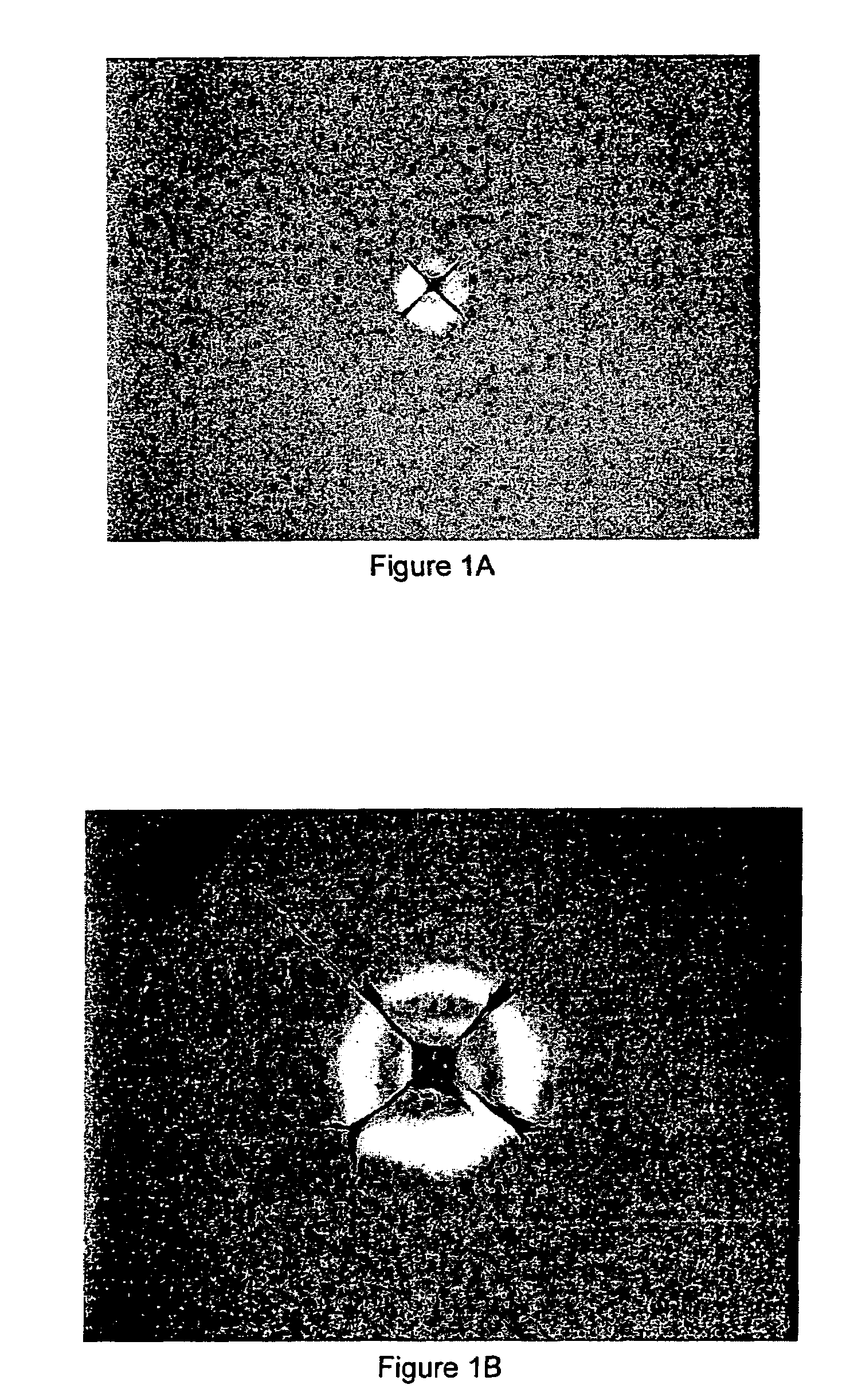
CDO materials with inferior mechanical properties will tend to have adhesive failures (delamination) and cohesive failures (cracking) during the copper-low k integration and packaging steps.
These failures are exacerbated by the increasing complexity of integrated circuits and frequently manifest with growing numbers of metallization layers.
However, film hardness is not the only measure used to determine whether a film is acceptable for use in chip integration.

Method used


Image

  • Methods for improving the cracking resistance of low-k dielectric materials
  • Methods for improving the cracking resistance of low-k dielectric materials
  • Methods for improving the cracking resistance of low-k dielectric materials

Examples


experimental examples

Example 1

[0056]A CDO film is prepared using a TMCTS+CO2 process. The film produced has a k value at 2.70. The film is then subjected to an UV light treatment.

[0057]FIGS. 4a and 4b show FTIR spectra of k2.7 film before and after UV treatment. FIG. 4a shows the spectra from 450 cm−1 to 4000 cm−1, detailing all the main peaks for a typical CDO film. FIG. 5b shows detailed peak variations for the Si—CH3 peak and the Si—CH2—Si peak.

[0058]After UV the treatment, the FTIR spectrum indicates a significant change in the Si—O peak at 1000 to 1150 cm−1. Also, significantly, the Si—CH3 peak has decreased and Si—CH2—Si has increased as a result of the UV treatment, which indicates that the UV treatment has induced some Si—CH3 bond dissociation and crosslinking.

[0059]The film bond structure change is also indicated by a change in refractive index (RI) at 633 nm (not shown). This is because increased crosslinking densifies the film and an increased in Si—C bond concentration increases the RI. For ...


PUM

PropertyMeasurementUnit
Temperatureaaaaaaaaaa
Lengthaaaaaaaaaa

Abstract

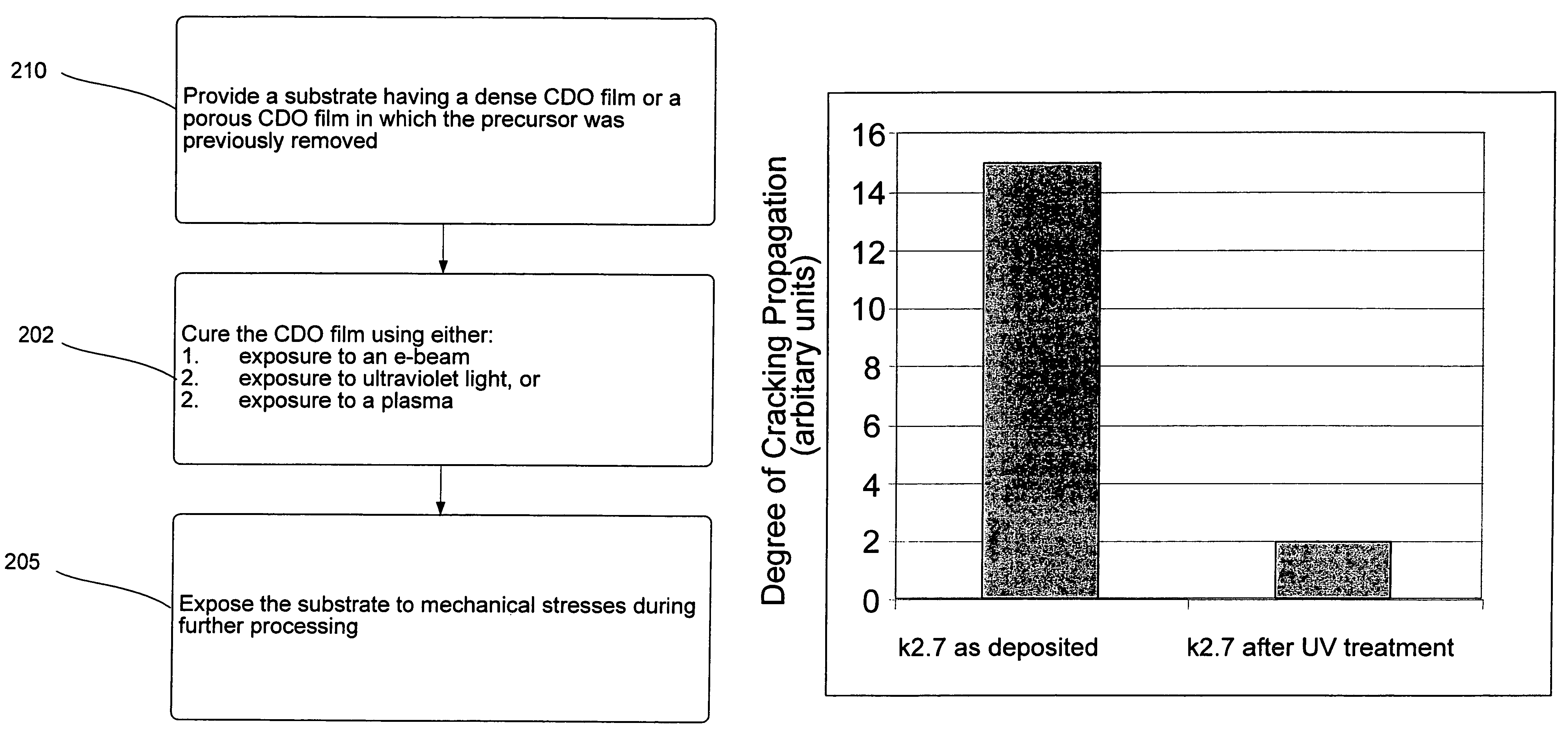
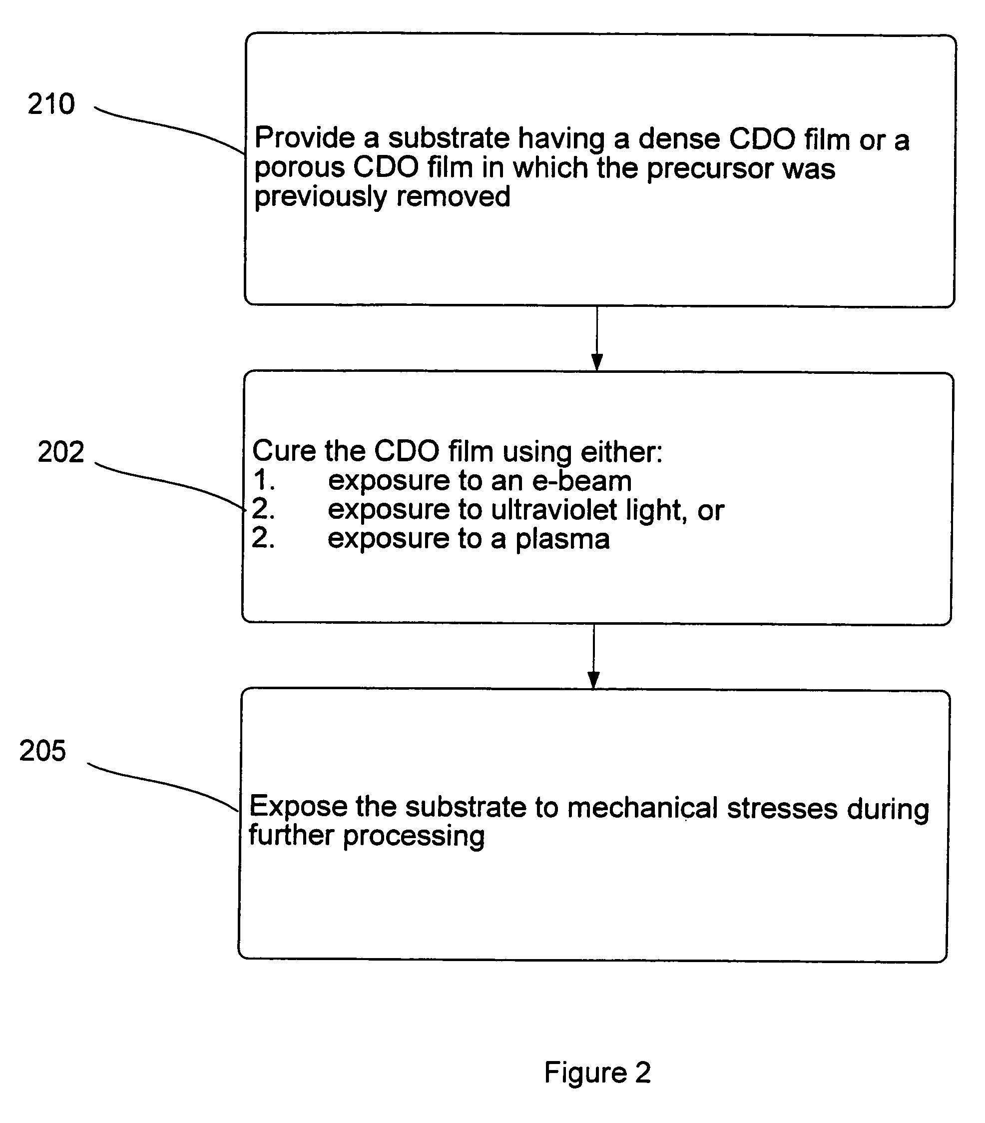
Methods for improving the mechanical properties of a CDO film are provided. The methods involve, for instance, providing either a dense CDO film or a porous CDO film in which the porogen has been removed followed by curing the CDO film at an elevated temperature using either a UV light treatment, an e-beam treatment, or a plasma treatment such that the curing improves the mechanical toughness of the CDO dielectric film.

Description

CROSS-REFERENCE TO RELATED APPLICATIONS[0001]This application is a divisional application of and claims priority from U.S. patent application Ser. No. 10 / 860,340, filed on Jun. 2, 2004 now U.S. Pat. No. 7,094,713, titled “Methods for Improving the Cracking Resistance of Low-k Dielectric Materials,” by Niu et al.; which is in turn, a continuation-in-part of U.S. patent application Ser. No. 10 / 807,680, filed on Mar. 23, 2004, titled “Methods of Porogen Removal for Porous Low Dielectric Constant Films Using Plasma Treatments,” by Wu et al., which is in turn, a continuation-in-part of U.S. patent application Ser. No. 10 / 800,377, filed on Mar. 11, 2004 now abandoned, titled “Method and Apparatus for UV Exposure of Low Dielectric Constant Materials for Porogen Removal and Improved Mechanical Properties,” by Srinivasan et al. Both applications are incorporated herein by reference in their entireties and for all purposes.FIELD OF THE INVENTION[0002]This invention relates to methods for prep...

Claims


Application Information

Patent Timeline
IPC IPC(8): H01L21/26H01L21/76
CPCC23C16/401C23C16/56H01L21/02126H01L21/02216H01L21/02274H01L21/0234H01L21/02348H01L21/02351H01L21/3105H01L21/31633H01L21/31695H01L21/02203
Inventor NIU, DONGFU, HAIYINGLU, BRIANWANG, FENG
Owner NOVELLUS SYSTEMS
Learn More