Band-structure modulation of nano-structures in an electric field

a technology of band structure and electric field, applied in the field of nanostructures, can solve the problems of insufficient satisfaction of none of these devices, the downsizing of integrated circuits is reaching its limits,

Inactive Publication Date: 2008-06-10
THE BOARD OF TRUSTEES OF THE LELAND STANFORD JUNIOR UNIV
View PDF23 Cites 47 Cited by
  • Summary
  • Abstract
  • Description
  • Claims
  • Application Information

AI Technical Summary

Benefits of technology

[0008]One effect of altering the energy band structure or gap of the elongated nano-structure is to cause a change in the electrical conductance of the nano-structure. In response to the electric field applied, electrical charge on the nano-structure can be redistributed without changin

Problems solved by technology

However, due to physical limitations, such downsizing of integrated circuits is reaching its limits.
While the above-descr

Method used


Image

  • Band-structure modulation of nano-structures in an electric field
  • Band-structure modulation of nano-structures in an electric field
  • Band-structure modulation of nano-structures in an electric field

Examples


Embodiment Construction

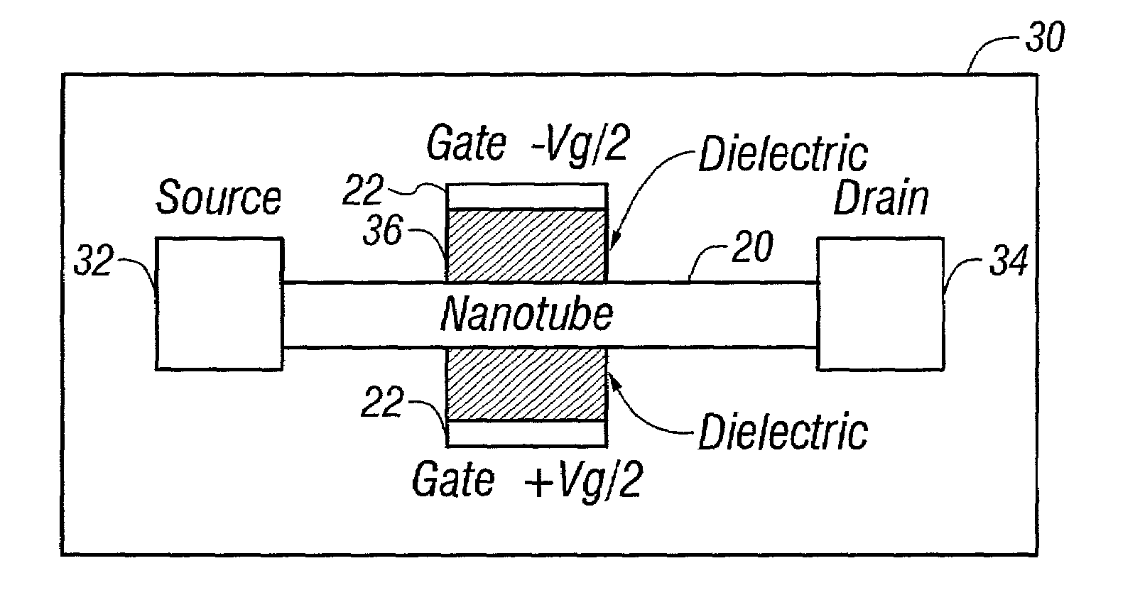
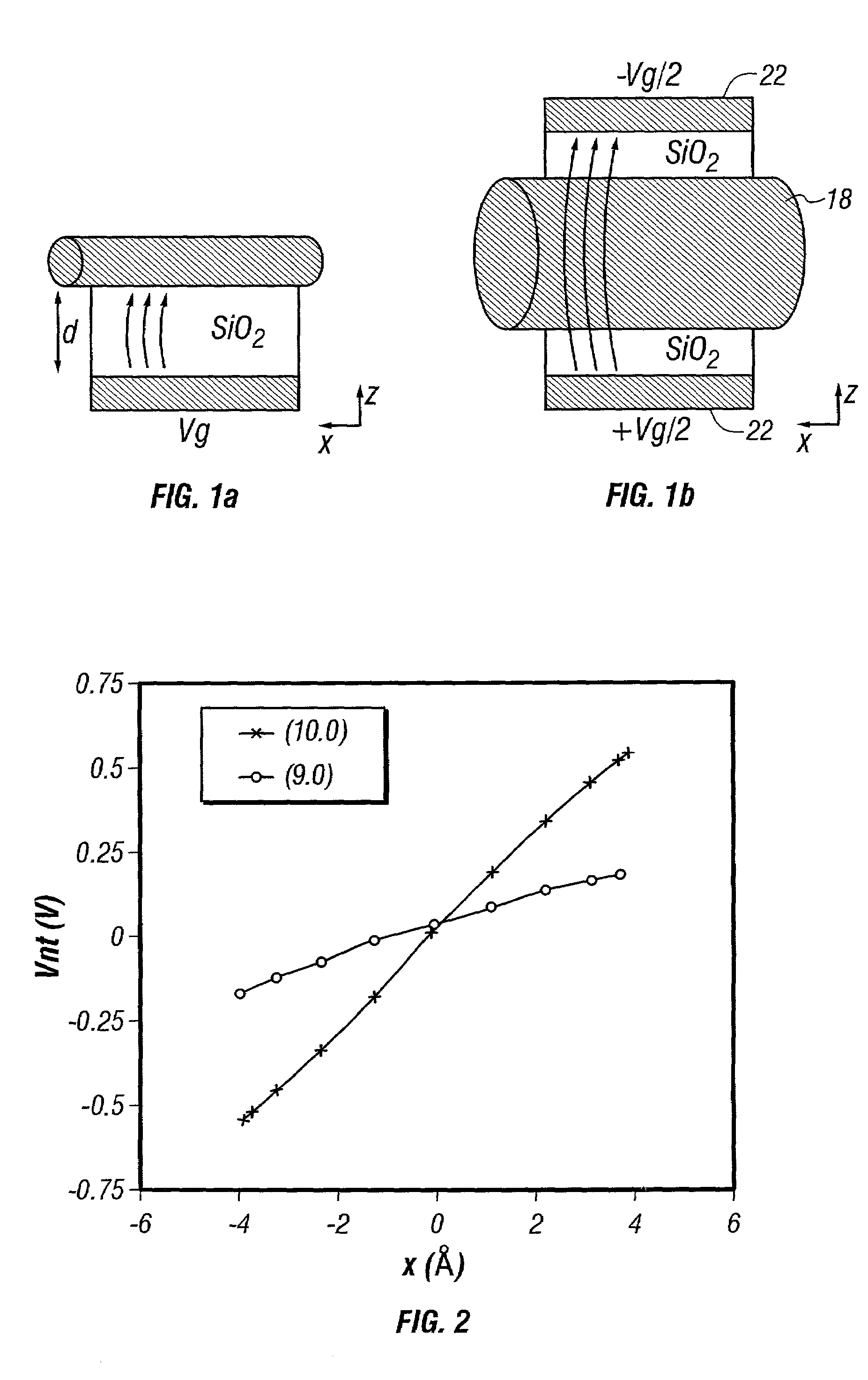
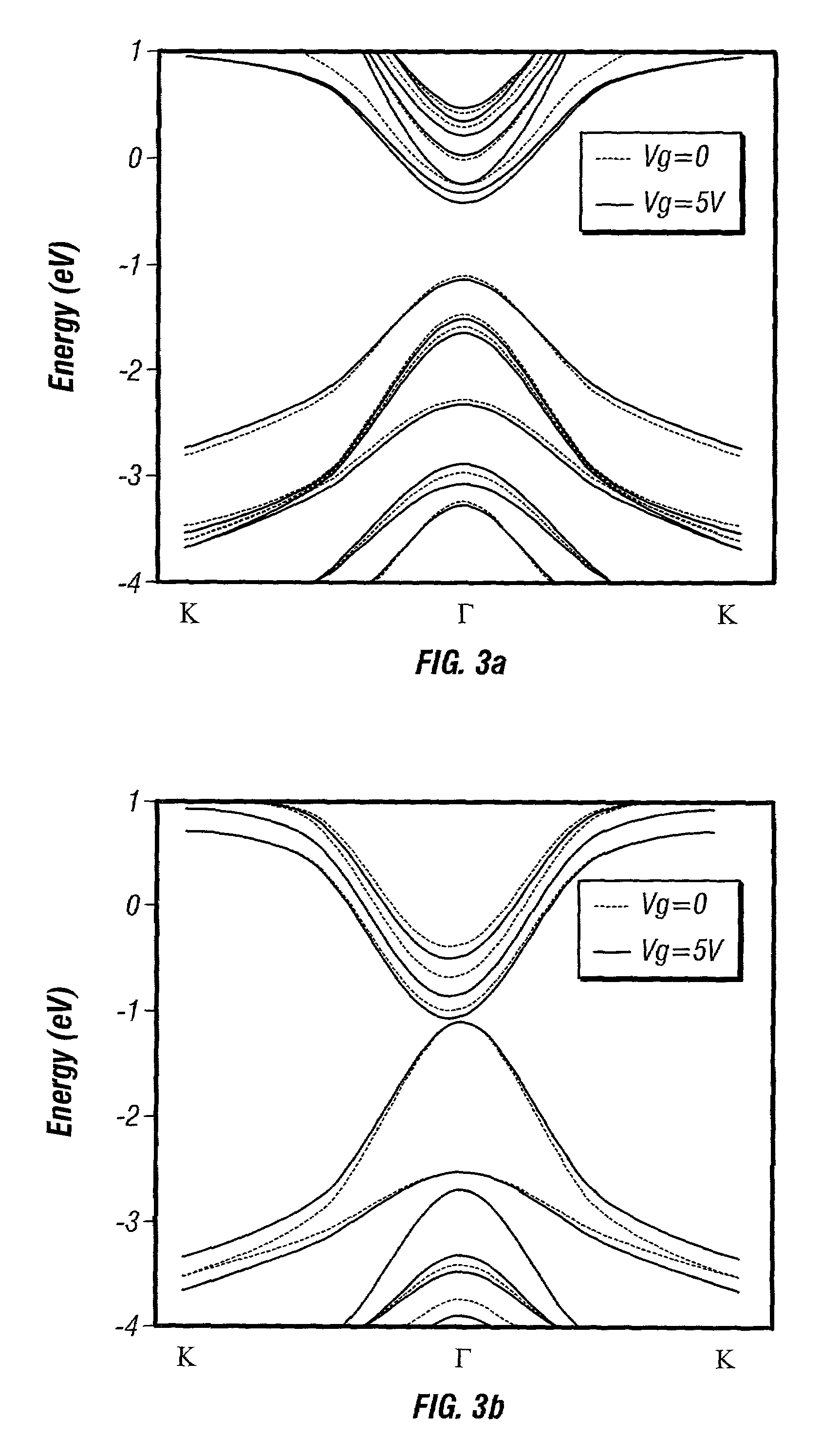
[0035]The structure in FIG. 1b illustrates the invention. This structure has two main differences from the conventional nanotube MOS capacitor model. Firstly, instead of being one of the capacitor electrodes the nanotube is placed in the center of the dielectric gap. In this way the capacitor (with plates 22) acts as a split-gate on the nanotube, with gate voltages of ±Vg / 2 respectively. Because of its position the fermi energy for the tube can be maintained at 0V in simulations. The advantage of this approach is that no net charge needs to enter the nanotube 18 to reach equilibrium, irrespective of the value of Vg so that the equilibrium can be reached faster. Secondly, the dielectric gap d is chosen to be similar to the nanotube diameter dt. This results in a considerable portion of Vg appearing as a potential gradient at the atom locations about the nanotube circumference. Where the tube 18 is not cylindrical, this gradient appears around the tube perimeter. Changes in the band-s...


PUM


Abstract

A method to electronically modulate the energy gap and band-structure of semiconducting carbon nanotubes is proposed. Results show that the energy gap of a semiconducting nanotube can be narrowed when the nanotube is placed in an electric field perpendicular to the tube axis. Such effect in turn causes changes in electrical conductivity and radiation absorption characteristics that can be used in applications such as switches, transistors, photodetectors and polaron generation. By applying electric fields across the nanotube at a number of locations, a corresponding number of quantum wells are formed adjacent to one another. Such configuration is useful for Bragg reflectors, lasers and quantum computing.

Description

BACKGROUND OF THE INVENTION[0001]This invention relates in general to nano-structures, and in particular to applications involving band-structure modulation of such structures in an electric field.[0002]Nowadays integrated circuits dominate electronics and have become one of the world's largest and most critical industries. The last few decades have seen a continual miniaturization of integrated circuits. However, due to physical limitations, such downsizing of integrated circuits is reaching its limits. The present scale of devices is on the order of tenths of microns. Nanometer scale devices have been proposed as a solution. One nanometer scale device that has been proposed is the carbon nanotube. Carbon nanotubes possess several interesting physical and electronic properties. Semi-conducting nanotubes have been grown up to several microns in length. In addition ohmic contacts to nanotubes have been demonstrated using Au and Pt electrodes. See, for example, the articles A. Bachtol...

Claims


Application Information

Patent Timeline
IPC IPC(8): H01L27/088H01L29/76G06N99/00H01L29/16H01L51/30
CPCB82Y10/00G06N99/002G11C13/025H01L29/16H01L29/7613H01L51/0048H01L51/0508H01L51/0512H01L51/428H01S5/125H01S5/18302G11C13/04G11C2213/17H01S5/0265H01S5/0614Y02E10/549Y10S977/755Y10S977/749G06N10/00H10K85/221H10K10/46H10K10/462H10K30/65
Inventor O'KEEFFE, JAMESCHO, KYEONGJAE
Owner THE BOARD OF TRUSTEES OF THE LELAND STANFORD JUNIOR UNIV
Why Eureka
Try Eureka