Surface acoustic wave device and electronic circuit device

a surface acoustic wave and electronic circuit technology, applied in the direction of semiconductor devices, electrical devices, electric/electrostrictive/magnetostrictive devices, etc., can solve the problem of difficult increase of the size of the mobile communication apparatus, and achieve the effect of reducing the mounting area and the number of laminations, and being sensitive and reliabl

Inactive Publication Date: 2008-06-10
KYOCERA CORP
View PDF5 Cites 24 Cited by
  • Summary
  • Abstract
  • Description
  • Claims
  • Application Information

AI Technical Summary

Benefits of technology

[0020]According to the surface acoustic wave device having such a configuration, when the surface acoustic wave device is mounted on the circuit board, an area to be covered with the insulator can be adjusted such that the partial area (exposed area) of the conductor pattern is overlapped with a connecting conductor formed on the circuit board depending on the position of the connecting conductor formed on the circuit board. Consequently, the position of the connecting conductor formed on the circuit board can be freely set. Consequently, the versatile surface acoustic wave device can be provided.
[0039]In the electronic circuit device comprising the surface acoustic wave device, it is preferable that phase matching means for matching the phases of signals passing through the plurality of surface acoustic wave elements is provided on the circuit board. According to this configuration, the surface acoustic wave device does not contain the phase matching means, thereby making it possible to reduce the mounting area and the number of laminations in the surface acoustic wave device. Therefore, there can be provided a microminiature and low-height electronic circuit device having passbands of different frequencies.

Problems solved by technology

However, the size of the mobile communication apparatus is difficult to increase from a request of the market.

Method used


Image

  • Surface acoustic wave device and electronic circuit device
  • Surface acoustic wave device and electronic circuit device
  • Surface acoustic wave device and electronic circuit device

Examples


first embodiment

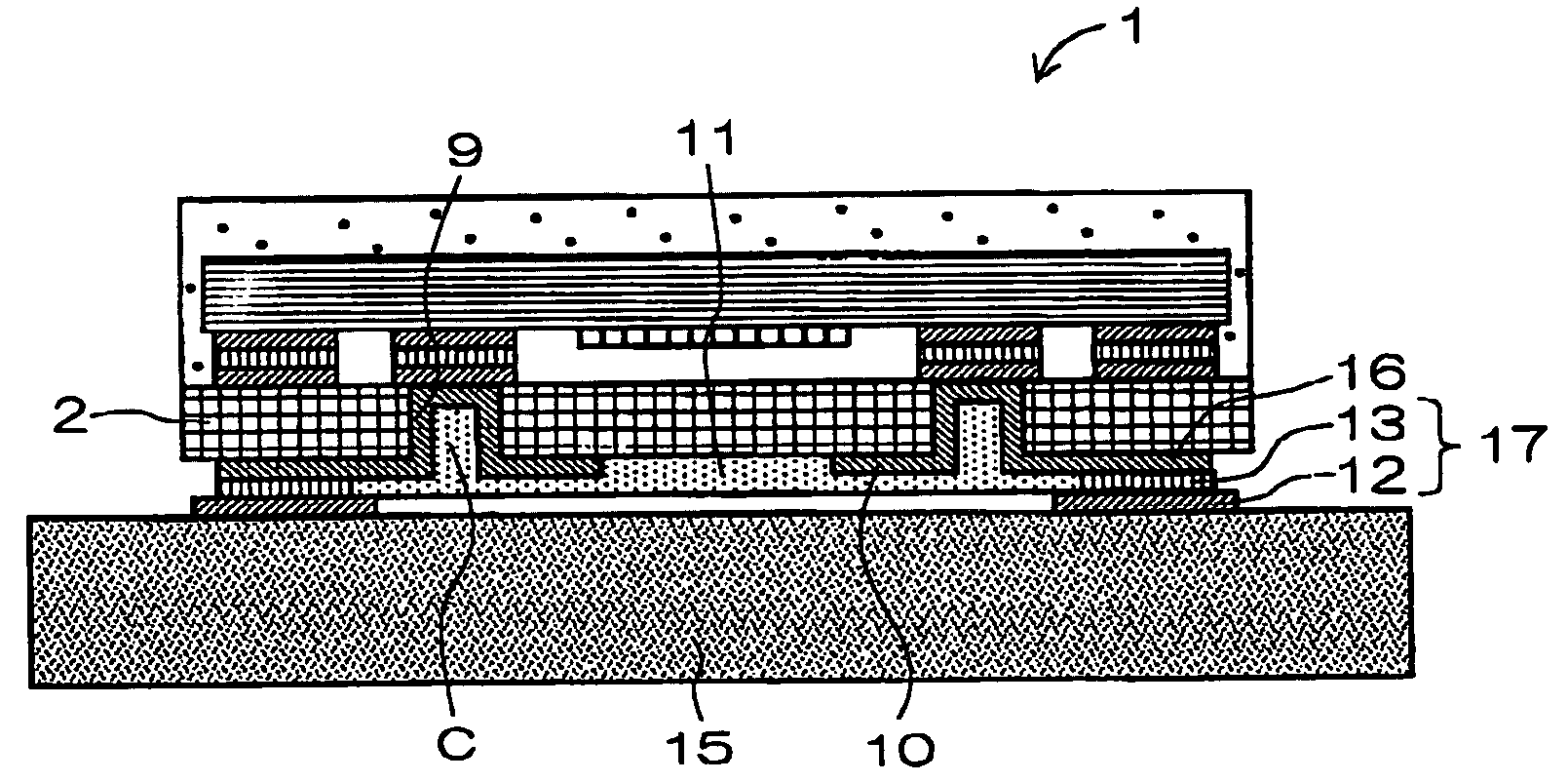
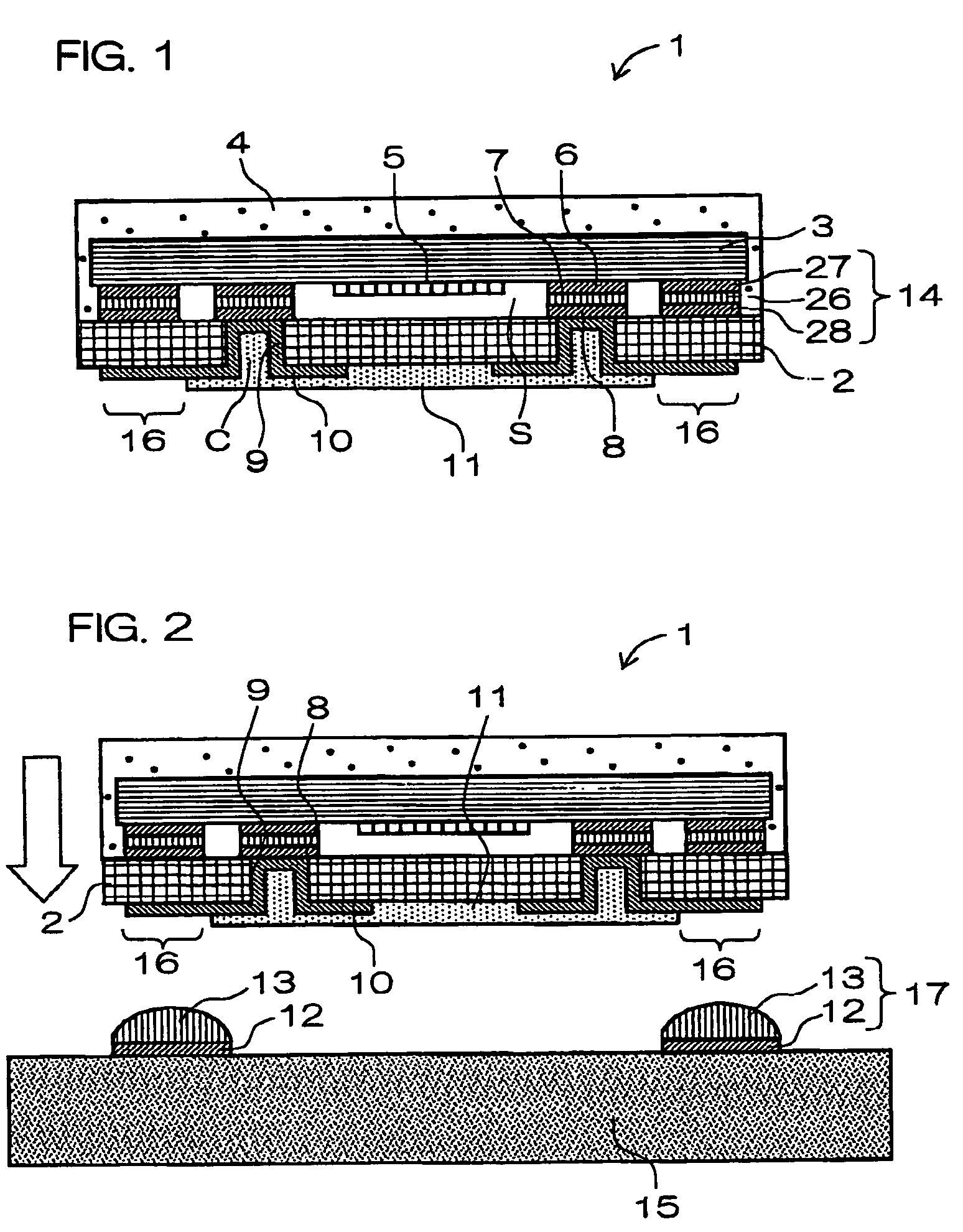
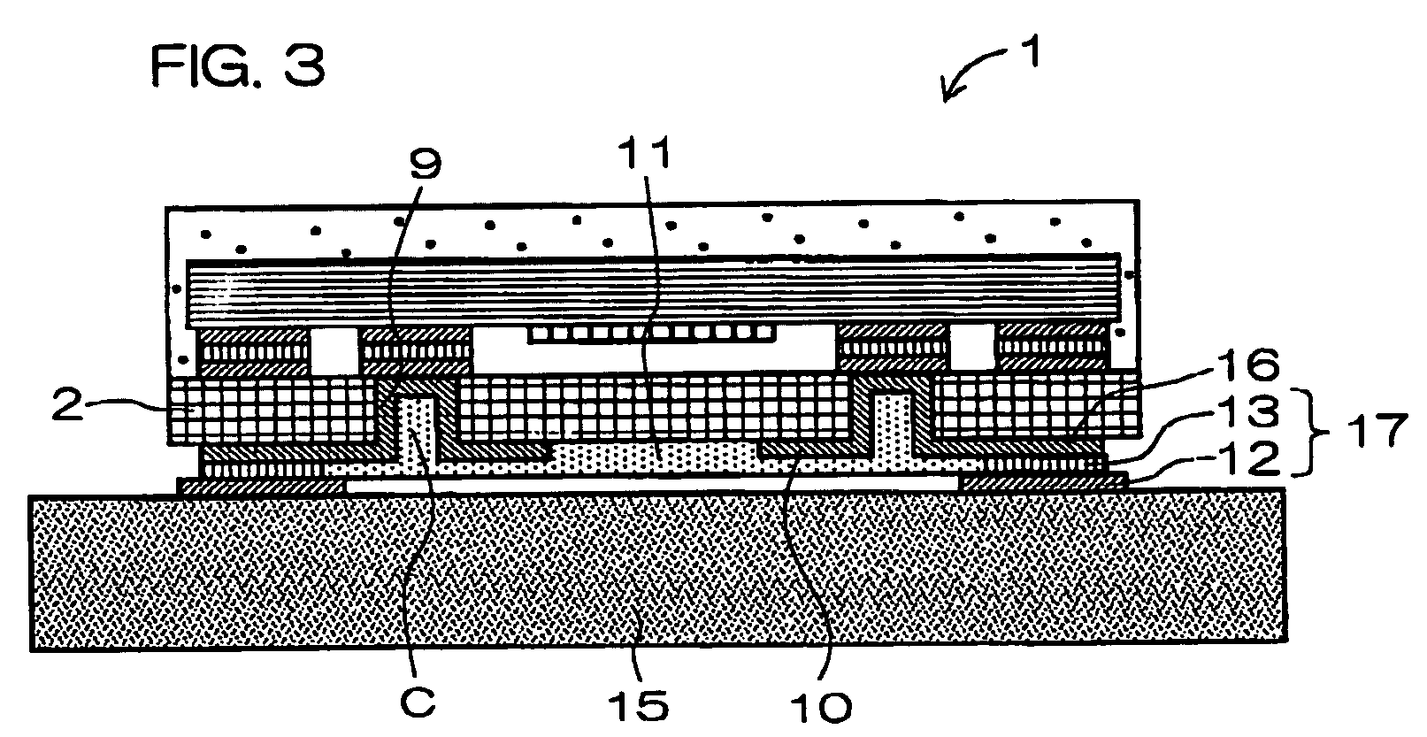
[0056]FIG. 1 is a cross-sectional view showing a surface acoustic wave device 1 according to the present invention. FIGS. 2 and 3 are cross-sectional views showing the steps of mounting the surface acoustic wave device 1 on a circuit board 15 in an electronic circuit device to configure the electronic circuit device.

[0057]As shown in FIG. 1, the surface acoustic wave device 1 comprises a piezoelectric substrate 3 and a mounting base member 2.

[0058]An excitation electrode 5 formed of an IDT (Inter Digital Transducer) electrode and a signal electrode 6 connected to the excitation electrode 5 (the connected state is not illustrated because of a cross-sectional view) are formed on one main surface of the piezoelectric substrate 3. The piezoelectric substrate 3, the excitation electrode 5, and the signal electrode 6 form a surface acoustic wave element. The excitation electrode 5 and the signal electrode 6 are generically referred to as a “surface acoustic wave element electrode”.

[0059]A...

examples

[0095]Specific examples of the present invention will be described while referring to the drawings.

[0096]The surface acoustic wave device shown in FIG. 1 was fabricated.

[0097]An Al (99 mass %)-Cu (1 mass %) IDT electrode pattern, an input-output electrode pattern, and a wiring pattern for electrically connecting them were formed on the piezoelectric substrate 3 which is a 38.7° Y-cut X-direction propagation lithium tantalate single crystal substrate.

[0098]A lithium tantalate wafer which is a substrate material was first ultrasonically cleaned by an organic solvent such as acetone or IPA (isopropyl alcohol), to clean an organic component. The substrate was then sufficiently dried by a clean oven.

[0099]In film formation of the electrode, a sputtering apparatus was employed, to form an Al—Cu film having the above-mentioned composition, a photoresist was then spin-coated to a thickness of approximately 0.5 μm, and the excitation electrode 5 was exposed to a desired electrode pattern by ...

second embodiment

[0114]A surface acoustic wave device according to another embodiment of the present invention will be described in detail while referring to the drawings.

[0115]FIG. 10 is a cross-sectional view showing a mounting structure of a surface acoustic wave device according to the present invention. FIG. 11 is a plan view of an electrode structure of a surface acoustic wave element provided in a piezoelectric substrate 3 in the surface acoustic wave device.

[0116]FIGS. 12 and 13 respectively illustrate an electrode structure on the side of a surface of a mounting base member 2 and an electrode structure on the side of a reverse surface of the mounting base member 2. The mounting base member 2 shown in FIG. 10 is illustrated in a cross-sectional view taken along a line X-X′ shown in FIG. 12.

[0117]As shown in FIGS. 10 and 11, in the surface acoustic wave device according to the present invention, a plurality of surface acoustic wave element electrodes (38 and 39 shown in FIG. 11) having passba...


PUM


Abstract

In a surface acoustic wave device, an excitation electrode 5 in a surface acoustic wave element is provided on a lower surface of a piezoelectric substrate 3, and the lower surface of the piezoelectric substrate 3 is disposed in a state where it is opposed to an upper surface of a mounting base member 2. The surface acoustic wave device comprises a through hole 9 penetrating between the upper surface and a lower surface of the mounting base member 2, a lead electrode 10 closing the through hole 9 and formed so as to extend to the lower surface of the mounting base member 2, and an insulator 11 covering the lead electrode 10 so as to expose its partial area 16. When the surface acoustic wave device is mounted on a circuit board or the like, therefore, the through hole 9 is closed by the insulator 11, so that no bubbles are produced in the through hole 9, and cracks can be prevented from appearing, thereby making it possible to provide a highly reliable surface acoustic wave device having no inferior connection or the like.

Description

BACKGROUND OF THE INVENTION[0001]1. Field of the Invention[0002]The present invention relates to a surface acoustic wave device having a so-called face down structure comprising a base member and a piezoelectric substrate having a surface acoustic wave element formed on its one main surface and configured by opposing the one main surface of the piezoelectric substrate to an upper surface of the base member, and an electronic circuit device in which the surface acoustic wave device is disposed on a circuit board.[0003]2. Description of the Related Art[0004]In recent years, surface acoustic wave filters have been widely utilized in a communication field, and particularly are frequently used for mobile communication apparatuses. The mobile communication apparatus has evolved to a multifunctional apparatus also having functions serving as a digital camera and a radio receiver and further the function of remotely controlling home electric appliances.[0005]In such flow, the number of devi...

Claims


Application Information

Patent Timeline
Patent Type & Authority Patents(United States)
IPC IPC(8): H03H9/00H03H9/10H03H3/08H03H9/02H03H9/25H03H9/64H03H9/72
CPCH03H9/0576H03H9/059H03H9/1085H03H9/725H03H9/02897H03H2250/00H01L2224/16225H01L2924/181H01L2924/00012
Inventor KOGA, WATARUYAMAGATA, YOSHIFUMINAGAMINE, SHIGEHIKO
Owner KYOCERA CORP
Why Eureka
Try Eureka