Radio-frequency switch circuit and semiconductor device

a radio frequency switch and semiconductor technology, applied in the direction of electronic switching, electrical equipment, pulse technique, etc., can solve the problems of high circuit cost and difficulty in using a material with a large sheet resistance in the semiconductor process, and achieve the effect of increasing the chip size and without a degradation in performan

Inactive Publication Date: 2008-06-24
COLLABO INNOVATIONS INC
View PDF18 Cites 66 Cited by
  • Summary
  • Abstract
  • Description
  • Claims
  • Application Information

AI Technical Summary

Benefits of technology

[0011]Therefore, an object of the present invention is to provide a small-size and high-performance radio-frequency switch circuit without a degradation in performance due to signal leakage and an increase in chip size, and a semiconductor device employing the radio-frequency switch circuit.
[0019]According to the above-described present invention, concerning the resistance values of a plurality of resistance elements connected to the gate electrodes of a plurality of field-effect transistors connected in series or a multigate field-effect transistor, only a resistance element connected to a gate electrode closest to an input / output terminal to which a radio-frequency signal is input is set to be a highest value. Thereby, the radio-frequency switch circuit of the present invention can have a significantly reduced footprint (chip size) on a semiconductor substrate while keeping the same performance as that of conventional radio-frequency switch circuits.

Problems solved by technology

However, it is difficult to use a material having a large sheet resistance in a semiconductor process.
Therefore, the chip size of the conventional radio-frequency switch circuit increases, resulting in high circuit cost.

Method used


Image

  • Radio-frequency switch circuit and semiconductor device
  • Radio-frequency switch circuit and semiconductor device
  • Radio-frequency switch circuit and semiconductor device

Examples


first embodiment

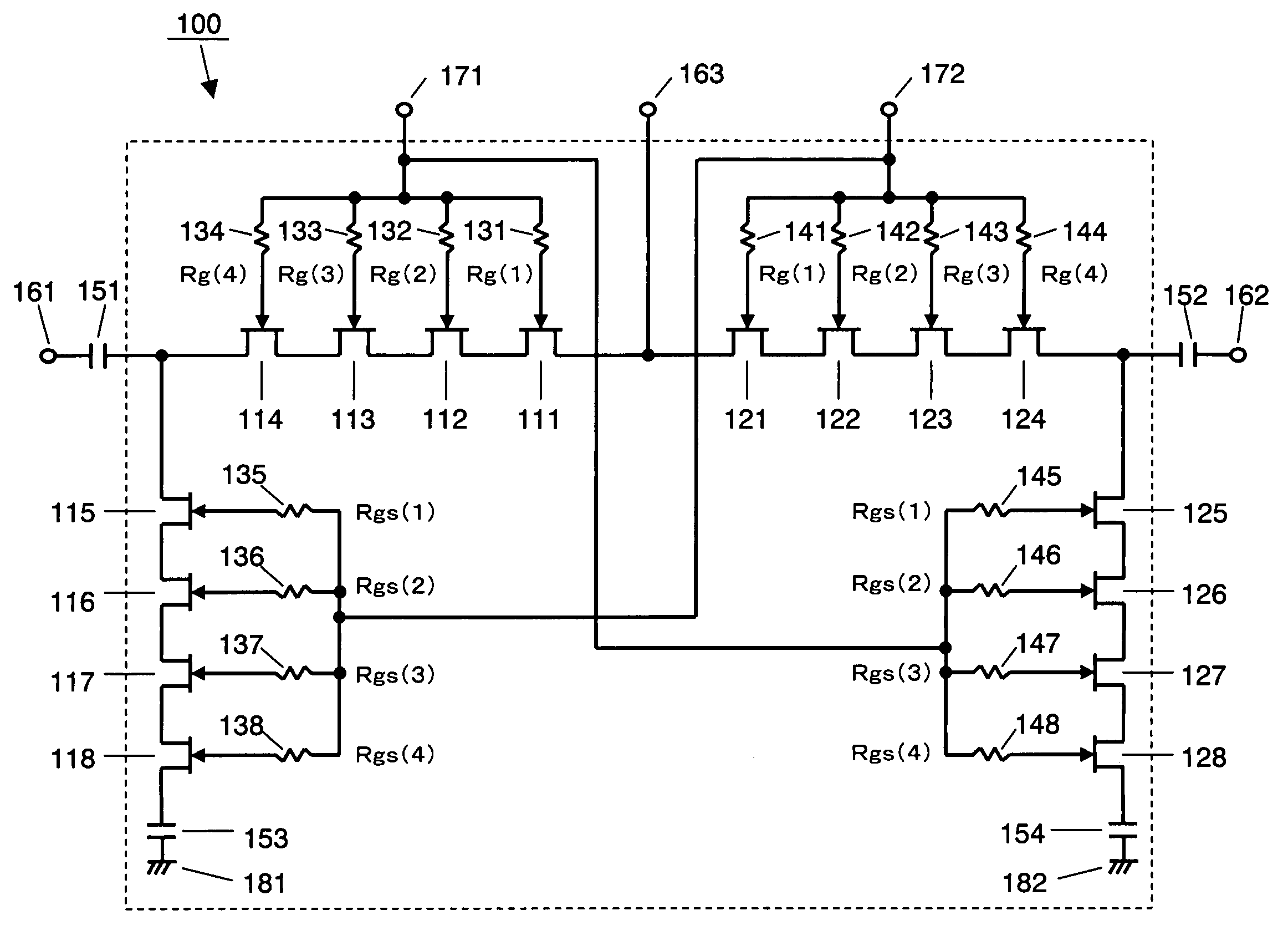
[0037]FIG. 1 is a diagram illustrating a radio-frequency switch circuit 100 according to a first embodiment of the present invention. The radio-frequency switch circuit 100 of FIG. 1 is composed of four groups of FETs connected in series, and functions as a Single Pole Double Throw (SPDT) circuit. The radio-frequency switch circuit 100 comprises FETs 111 to 118 and 121 to 128, gate bias resistors 131 to 138 and 141 to 148, capacitors 151 to 154, first to third input / output terminals 161 to 163, first and second control terminals 171 and 172, and ground terminals 181 and 182. The first to third input / output terminal 161 to 163 are terminals for inputting / outputting a radio-frequency signal.

[0038]In FIG. 1, the FETs 111 to 114 constitute a first switch section, and are connected in series between the third input / output terminal 163 and the first input / output terminal 161. The FETs 115 to 118 constitute a second switch section, and are connected in series between the first input / output...

second embodiment

[0057]FIG. 6 is a diagram illustrating a radio-frequency switch circuit 200 according to a second embodiment of the present invention. The radio-frequency switch circuit 200 of FIG. 6 is composed of four multigate FETs, and functions as an SPDT circuit. The radio-frequency switch circuit 200 comprises multigate FETs 211, 212, 221, and 222, gate bias resistors 231 to 238 and 241 to 248, capacitors 251 to 254, first to third input / output terminals 161 to 163, first and second control terminals 171 and 172, and ground terminals 181 and 182.

[0058]As can be seen from FIG. 6, the radio-frequency switch circuit 200 of the second embodiment of the present invention is different from the radio-frequency switch circuit 100 of the first embodiment of the present invention in that the first to fourth switch sections are each composed of one multigate FET. The multigate FET is known to have a plurality of gate electrodes (1a to 4a, 1b to 4b, 1c to 4c, and 1d to 4d in the example of FIG. 6), and ...


PUM


Abstract

Switch sections composed of a plurality of FETs 111 to 118 and 121 to 128 connected in series are provided between input / output terminals 161 and 162 and ground terminals 181 and 182, and between the input / output terminals 161 to 163. A plurality of gate bias resistors 131 to 138, 141 to 148 are also provided. One terminal of each gate bias resistor is connected to a gate electrode of a corresponding one of the FETs 111 to 118 and 121 to 128, while a control voltage 171 and 172 for switching an ON state and an OFF state of the switch section is applied to the other terminal. Among the FETs included in each switch section, concerning the FETs 114, 115, 124, and 125 to which signal power is applied when the switch section is in the OFF state, the gate bias resistors 134, 135, 144, and 145 connected to the gate electrodes are set to have a highest resistance value.

Description

BACKGROUND OF THE INVENTION[0001]1. Field of the Invention[0002]The present invention relates to a radio-frequency switch circuit and a semiconductor device, and more particularly, to a radio-frequency switch circuit employing a field-effect transistor, and a semiconductor device in which the radio-frequency switch circuit is integrated.[0003]2. Description of the Background Art[0004]In recent years, as performance of mobile communication apparatuses is improved, there is an increasing demand for small-sized and high-performance radio-frequency semiconductor devices. Particularly, low insertion loss and low distortion are simultaneously required for a radio-frequency switch circuit which performs antenna switching. Therefore, a method of constructing a radio-frequency switch circuit using a plurality of field-effect transistors (hereinafter referred to as “FETs”) connected together has been proposed.[0005]FIG. 12 is a diagram illustrating a conventional radio-frequency switch circui...

Claims


Application Information

Patent Timeline
Patent Type & Authority Patents(United States)
IPC IPC(8): H01P5/12H04B1/44
CPCH01P1/15H03K17/6871H03K17/693
Inventor NAKATSUKA, TADAYOSHIMIYAGI, MASASHI
Owner COLLABO INNOVATIONS INC
Why Eureka
Try Eureka