

Simple signal transmission circuit capable of decreasing power consumption
a transmission circuit and simple technology, applied in the direction of dc level restoring means or bias distortion correction, pulse technique, instruments, etc., can solve the problems of large power consumption, large power consumption, and high speed signal transmission circuits, and achieve the effect of reducing power consumption
- Summary
- Abstract
- Description
- Claims
- Application Information
AI Technical Summary
Benefits of technology
Problems solved by technology
Method used
Image


Examples
first embodiment
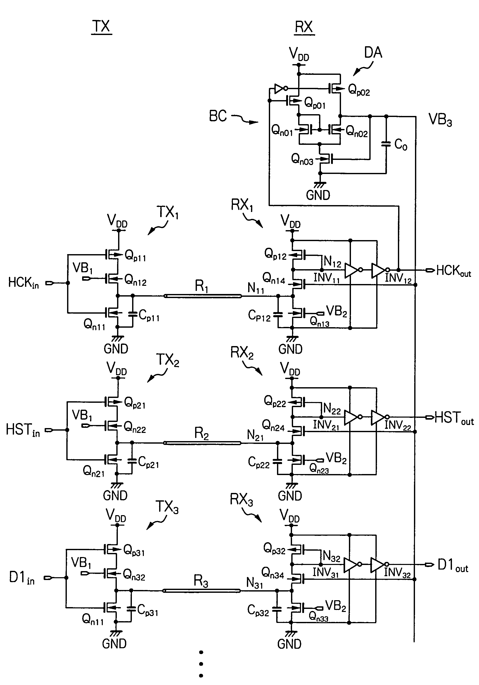
[0054]In FIG. 6, which illustrates the signal transmission circuit according to the present invention, a transmitter TX1 for receiving a horizontal clock signal HCKin is constructed by a CMOS inverter formed by a P-channel MOS transistor Qp11 and an N-channel MOS transistor Qn11 and a voltage amplitude limiting N-channel MOS transistor Qn12 connected between the transistors Qp11 and Qn11. In this case, a definite bias voltage VB1 is applied to the gate of the transistor Qn12 to limit a high level of an output signal. For example, the high level of the output signal is limited by about 1V lower than a power. supply voltage VDD such as 2.5V. Also, a receiver RX1 for receiving the horizontal clock signal HCKin to generate a horizontal clock signal HCKout is constructed by a load drain-gate connected P-channel MOS transistor Qp12, a constant current source formed by an N-channel MOS transistor Qn13 whose gate receives a definite bias voltage VB2, and a voltage adjusting N-channel MOS tr...
second embodiment
[0067]In FIG. 8, which illustrates the signal transmission circuit according to the present invention, a transmitter TX1′ for receiving a horizontal clock signal HCKin is constructed by a CMOS inverter formed by a P-channel MOS transistor Qp11′ and an N-channel MOS transistor Qn11′ and a voltage amplitude limiting P-channel MOS transistor Qp12′ connected between the transistors Qp11′ and Qn11′. In this case, a definite bias voltage VB1′ is applied to the gate of the transistor Qp12′ to limit a low level of an output signal. For example, the low level of the output signal is limited by about 1.5V higher than a ground voltage GND such as 0V. Also, a receiver RX1′ for receiving the horizontal clock signal HCKin to generate a horizontal clock signal HCKout is constructed by a load drain-gate connected N-channel MOS transistor Qn12′, a constant current source formed by a P-channel MOS transistor Q13′ whose gate receives a definite bias voltage VB2′, and a voltage adjusting P-channel MOS ...
PUM
| Property | Measurement | Unit |
|---|---|---|
| frequency | aaaaa | aaaaa |
| current | aaaaa | aaaaa |
| threshold voltage | aaaaa | aaaaa |
Abstract
Description
Claims
Application Information