
Semiconductor integrated circuit for high frequency power amplifier and electric components with the semiconductor integrated circuit

a technology of integrated circuits and semiconductors, applied in the direction of automatic tone/bandwidth control, transmission, gain control, etc., can solve the problems of inability to control power, inability to implement power control, deterioration of precision, etc., and achieve high precision

Active Publication Date: 2008-07-01
MURATA MFG CO LTD
View PDF6 Cites 14 Cited by
  • Summary
  • Abstract
  • Description
  • Claims
  • Application Information

AI Technical Summary

Benefits of technology

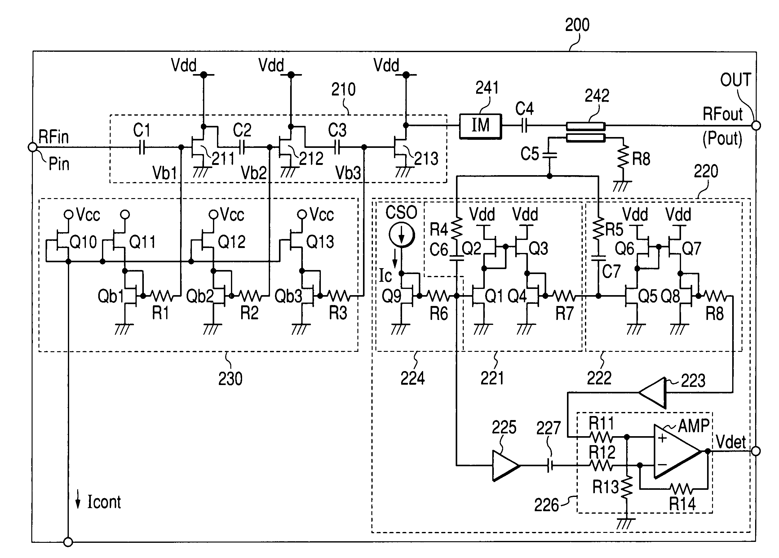
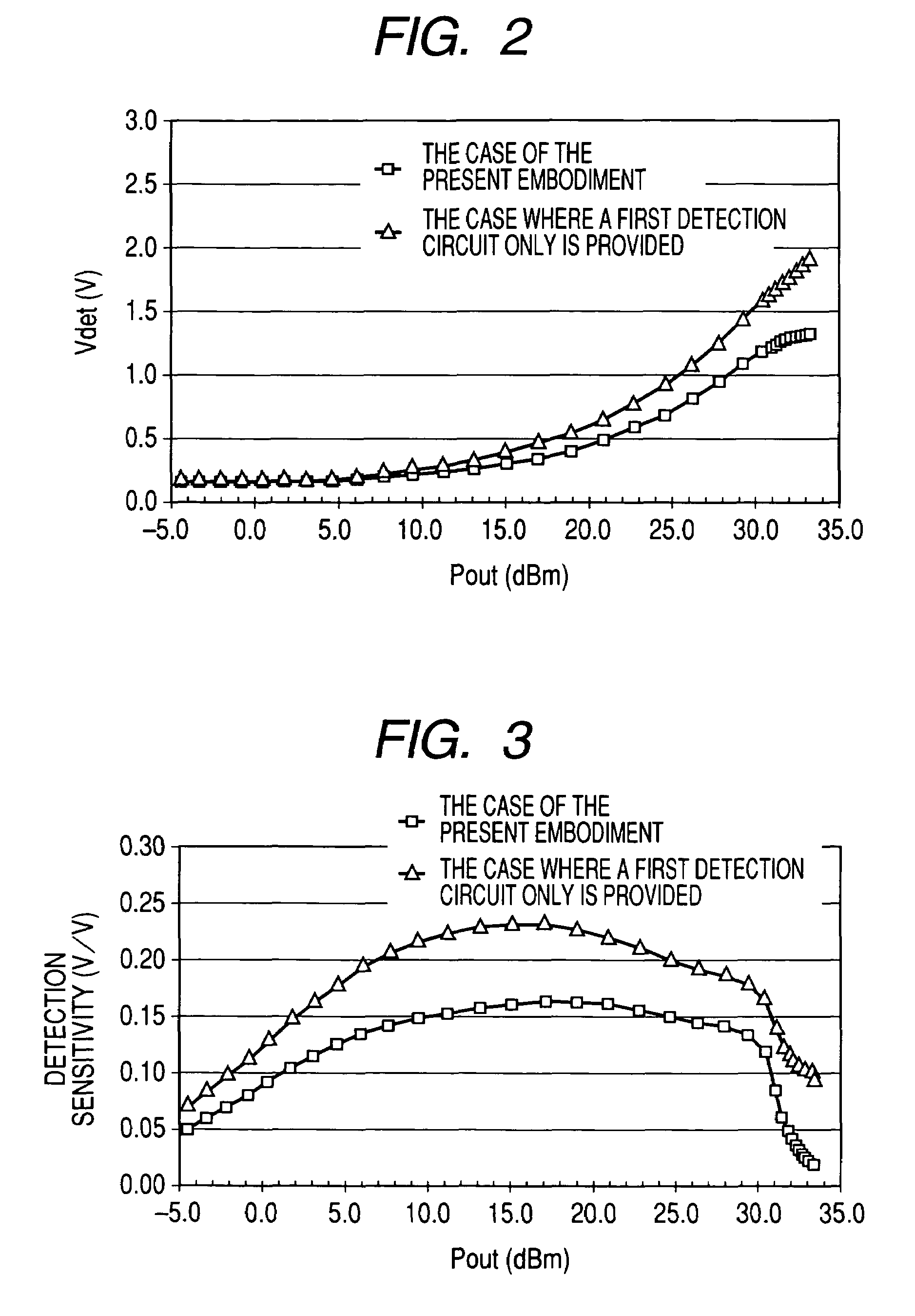
The present invention provides a semiconductor integrated circuit for high frequency power amplifier that can execute feedback control of output power with high precision by raising detection sensitivity of an output power detection circuit in a low output level region. The circuit is made up of two detection circuits capable of detecting an output signal, respectively, consisting of a first detection circuit and a second detection circuit, the second detection circuit is configured so as to have lower detection sensitivity than the first detection circuit in the low output level region. The first detection circuit is set so as to have higher detection sensitivity in the low output level region while the second detection circuit is set so as to become saturated at an earlier point in time than the first detection circuit when the output level is controlled to be gradually increased. The invention solves the problem of incapability of implementing power control as desired in a wireless communication system for executing the feedback control of the output power by detecting the output level.

Problems solved by technology

As a result, it has become evident that if sensitivity is set such that control sensitivity in a high output level region becomes optimum, control sensitivity in a low output level region becomes low, resulting in deterioration of precision while if sensitivity is set such that the control sensitivity in the low output level region becomes optimum, the control sensitivity in the high output level region becomes too high, so that the output of a detection circuit becomes saturated in the high output level region, thereby rendering it impossible to control power.
When detection of output power, for feedback control of the output level, is executed by the current detection circuit of the current detection scheme described as above, in a system of the Pin control scheme, it has become evident that there exists a problem of incapability of implementing power control as desired because the control sensitivity in the low output level region is low, and a sufficient detection voltage cannot be obtained even if the technology according to the previous application (JP-A No. 140518 / 2004) is applied.
However, in the case where the detection circuit with low sensitivity, and the detection circuit with high sensitivity are provided in parallel as described, there exists a problem in that abrupt variations in step and tilt occur at points of changeover in output of the two detection circuits, thereby rendering it impossible to implement smooth control of the output level.

Method used


Image

  • Semiconductor integrated circuit for high frequency power amplifier and electric components with the semiconductor integrated circuit
  • Semiconductor integrated circuit for high frequency power amplifier and electric components with the semiconductor integrated circuit
  • Semiconductor integrated circuit for high frequency power amplifier and electric components with the semiconductor integrated circuit

Examples


Embodiment Construction

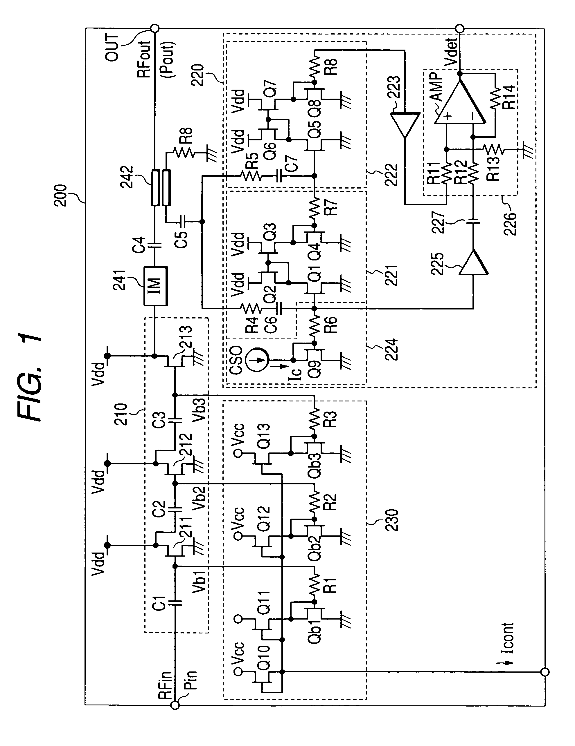
[0032]Preferred embodiments of the invention are described hereinafter with reference to the accompanying drawings.

[0033]FIG. 1 shows one embodiment of a high frequency power amplifier circuit (hereinafter referred to as a power module) with an output power detection circuit applied thereto, according to the invention. In the present specification, it is to be pointed out that a device with a configuration in which a plurality of semiconductor chips and discrete components are mounted on an insulation board, such as a ceramic board, with printed wiring provided on the surface, and inside, thereof, such that respective components are connected with each other so as to fulfill respective predetermined functions, thereby being enabled to be handled as if one electronic component, is referred to as a module.

[0034]A power module 200 according to the present embodiment comprises a high frequency power amplification unit 210 including amplifier FETs for amplifying an input high frequency s...


PUM


Abstract

In a high frequency power amplifier circuit in which bias voltages are applied to the transistors for amplification by current mirroring, The power amplifier includes a detection circuit including a transistor for detection which receives the AC component of an input signal to the last-stage transistor for amplification at its control terminal, a current mirror circuit which mirrors current flowing through that transistor, and a current-voltage converter which converts current flowing in the slave side of the current mirror circuit into a voltage. In the detection circuit, a voltage from a bias circuit for generating the bias voltages for the transistors for amplification is applied to the control terminal of the transistor for detections, and output of the detection circuit is applied to the control terminal of the last-stage transistor for amplification.

Description

CROSS-REFERENCE TO RELATED APPLICATION[0001]The present application claims priority from Japanese paten application No. 2004-276260 filed on Sep. 24, 2004, the content of which is hereby incorporated by reference into this application.BACKGROUND OF THE INVENTION[0002]The invention relates to a technology effective for application to a high frequency power amplifier circuit used in a wireless communication system, such as a cellular phone, and so forth, for amplifying a high frequency transmitting signal to be subsequently outputted, and electronic components with the same mounted therein, and more particularly, to a technology effective for application to an output power detection circuit for executing detection of an output level, necessary for feedback control of an output power.[0003]In general, a high frequency power amplifier circuit for amplifying modulated signals is assembled in an output unit on the sending side of a wireless communication equipment (mobile communication eq...

Claims


Application Information

Patent Timeline
Patent Type & Authority Patents(United States)
IPC IPC(8): H01Q11/12
CPCH03G3/3047H03G3/3042
Inventor AKAMINE, HITOSHITSUCHIYA, MASAHIROTAKAHASHI, KYOICHIKOSHIO, KAZUHIRO
Owner MURATA MFG CO LTD
Learn More