
Producing method of wired circuit board

a production method and wired circuit technology, applied in the direction of circuit masks, instruments, photomechanical apparatus, etc., can solve the problems of air bubbles entering the photosensitive solder resist and the protecting film, the disadvantage of the subsequent development process, and the elongation of the base material conveyed with the rollers

Inactive Publication Date: 2008-07-08
NITTO DENKO CORP
View PDF19 Cites 0 Cited by
  • Summary
  • Abstract
  • Description
  • Claims
  • Application Information

AI Technical Summary

Benefits of technology

The present invention provides a method for producing a wired circuit board that can prevent meandering of the elongate base material conveyed with rolls and also prevent entry of air bubbles in between a light-transparency protecting film and a photosensitive solder resist layer when the light-transparency protecting film is laminated on the photosensitive solder resist layer. This is achieved by providing a stiffener sheet on the elongate base material to cover the conductive pattern and forming a photosensitive solder resist layer on the surface of the elongate base material to cover the conductive pattern. The elongate base material can be bent flexibly at the both widthwise end portions to allow the photosensitive solder resist layer to be away from coating means for the photosensitive solder resist. This ensures reliable conveyance of the elongate base material even when the photosensitive solder resist layer is coated over the surface of the elongate base material while the elongate base material is conveyed with rolls. The method also includes laminating a light-transparency protecting film on the surface of the photosensitive solder resist layer and exposing the photosensitive solder resist layer to light through the light-transparency protecting film to prevent entry of air bubbles and scattering of light in the subsequent exposure process.

Problems solved by technology

However, when the conductive pattern is formed on the base material by the electrolytic plating, the following problems occur.
When this elongate base material is coated with the photosensitive solder resist to cover the conductive pattern by the roll coater, the conductive pattern formed to have a larger thickness at the both widthwise end portions of the elongate base material is brought into contact with the roll coater, to cause meander of the elongate base material conveyed with the rollers disadvantageously.
When the conductive pattern has a larger thickness at the both widthwise end portions of the elongate base material than at the widthwise central portion of the same, the pressure cannot be uniformly applied on the elongate base material including portions thereof close to the both ends thereof, to cause entry of air bubbles in between the photosensitive solder resist and the protecting film.
This will cause scattering of light in the subsequent exposure process, and as such can cause production of pinholes in the subsequent development process disadvantageously.

Method used


Image

  • Producing method of wired circuit board
  • Producing method of wired circuit board
  • Producing method of wired circuit board

Examples


example 1

[0088]A flexible wired circuit board was produced by the roll-to-roll process having the following processes and using the manufacturing equipment.

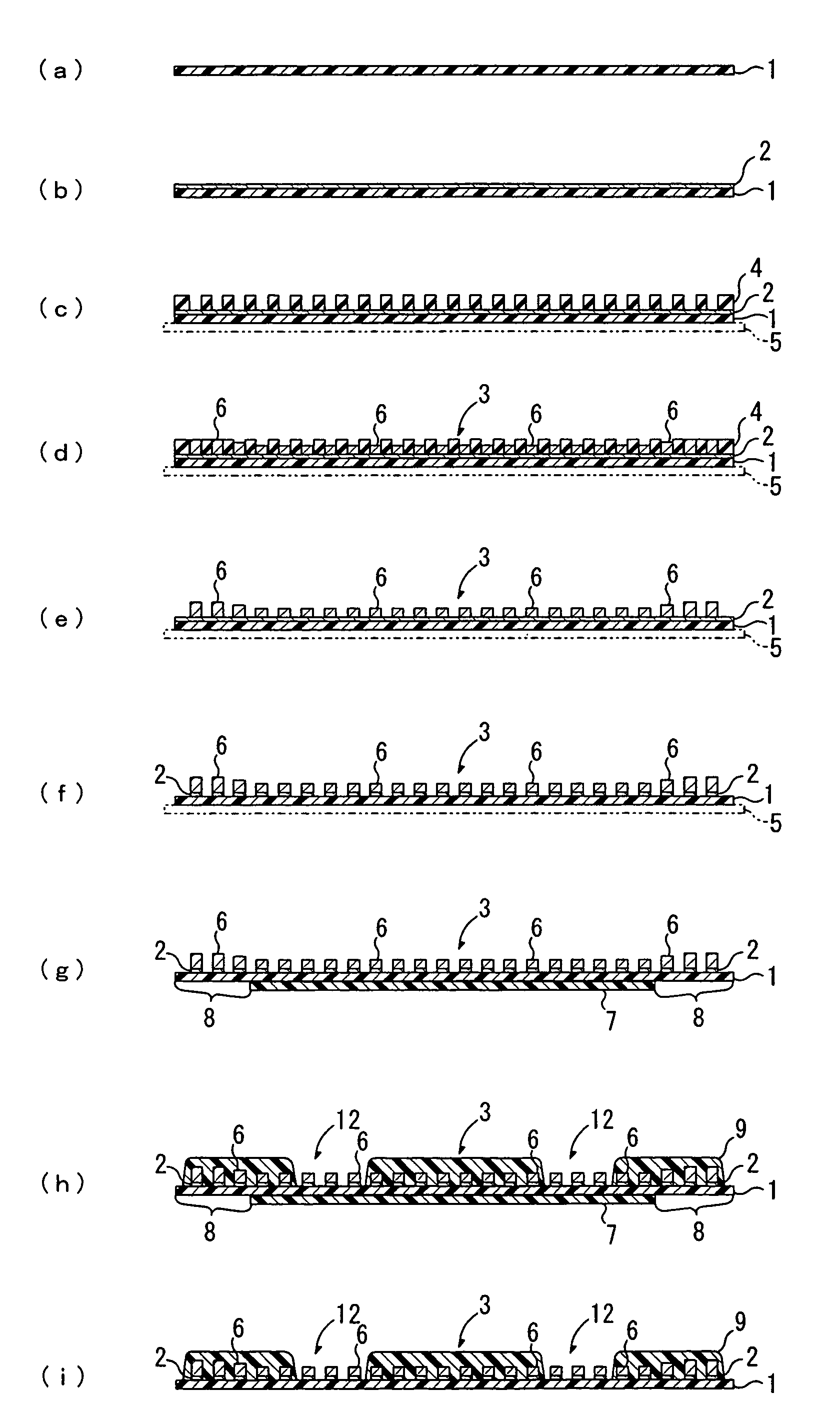
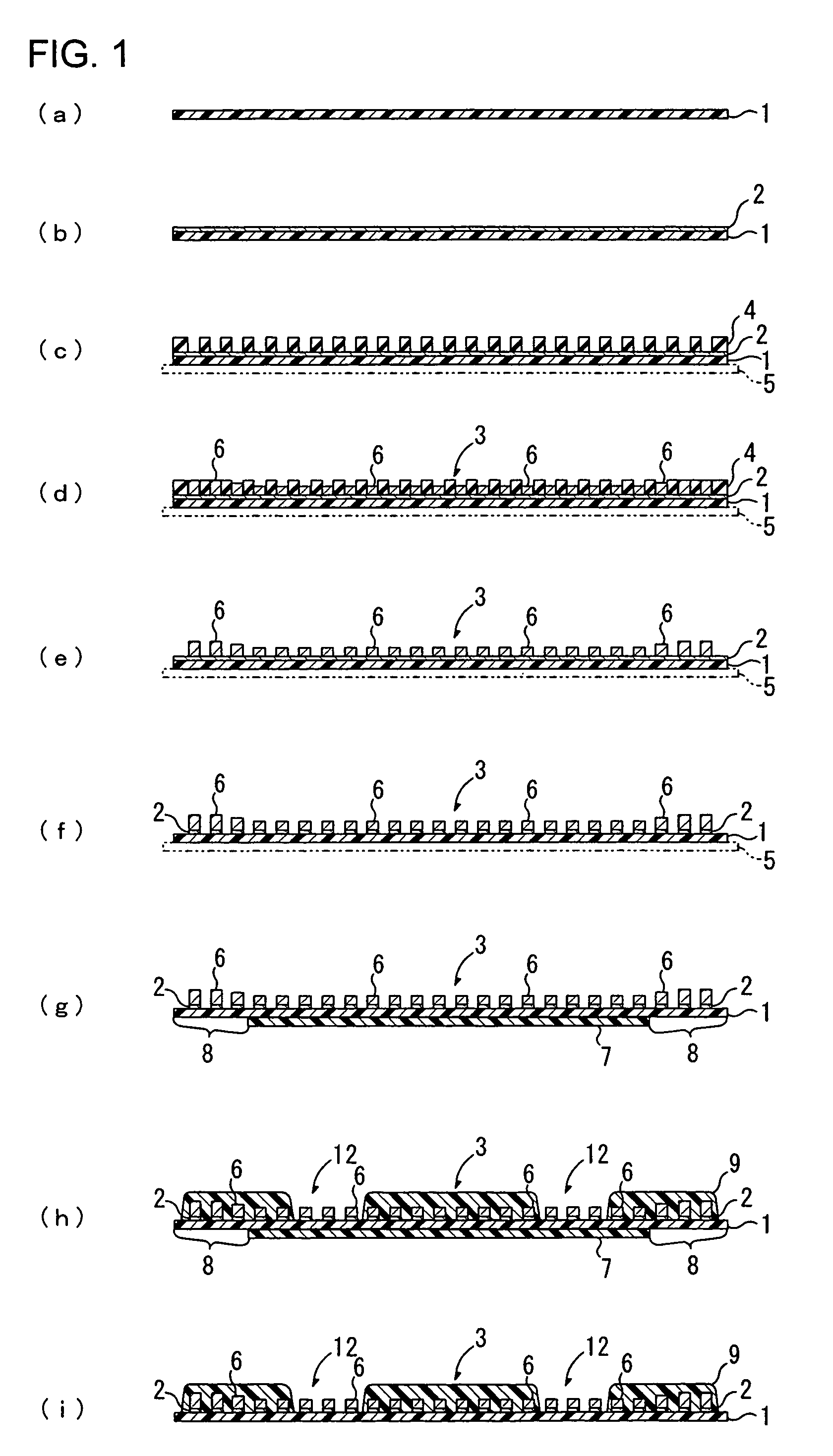
[0089]An elongate base material of a polyimide film having a width of 250 mm and a thickness of 25 μm was prepared (Cf. FIG. 1(a)). Then, a thin metal film comprising a thin chromium film having a thickness of 30 nm and a thin copper film having a thickness of 200 nm was sequentially formed on the entire surface of the elongate base material by the sputtering process (Cf FIG. 1(b)).

[0090]Then, at the same time as the adhesive bonding of a photosensitive dry film resist having a thickness of 20 μm to a surface of the thin metal film, a wide stiffener sheet of polyethylene terephthalate film with adhesive having a width of 252 mm and a thickness of 50 μm was adhesively bonded to the back side of the elongate base material. Thereafter, the photosensitive dry film resist was exposed to light and developed, to form a plating resist in a revers...


PUM

PropertyMeasurementUnit
thicknessaaaaaaaaaa
thicknessaaaaaaaaaa
lengthaaaaaaaaaa

Abstract

A producing method of a wired circuit board that can prevent meandering of the elongate base material conveyed with the rolls and also prevent entry of air bubbles in between a light-transparency protecting film and a photosensitive solder resist layer when the light-transparency protecting film is laminated on the photosensitive solder resist layer. After a conductive pattern 3 is formed on the front side of the elongate base material 1 by the additive process, a narrow stiffener sheet 7 smaller in width than the elongate base material 1 is provided on the back side of the elongate base material 1. Then, after the photosensitive solder resist layer 10 is formed on the front side of the elongate base material 1 to cover the conductive pattern 3, the light-transparency protecting film 11 is laminated on the front side of the photosensitive solder resist layer 10. Thereafter, the photosensitive solder resist layer 10 is exposed to light through the light-transparency protecting film 11. Then, after the light-transparency protecting film 11 is stripped off from the photosensitive solder resist layer 10, the photosensitive solder resist layer 10 was developed and then cured by heating. Thereafter, the narrow stiffener sheet 7 is stripped off from the elongate base material. The flexible wired circuit board is produced in the manner described above.

Description

BACKGROUND OF THE INVENTION[0001]1. Field of the Invention[0002]This application claims priority from Japanese Patent Appln. No. 2004-299254, filed Oct. 13, 2004, the contents of which are herein incorporated by reference in their entirety.[0003]The present invention relates to a producing method of a wired circuit board and, more particularly, to a method of producing a wired circuit board while conveying an elongate base material using rolls.[0004]2. Description of the Prior Art[0005]As is known, the roll-to-roll process is used for forming a conductive pattern and the like on a surface of elongate base material while conveying the elongate base material by using rolls, in order to provide an improved production efficiency of the wired circuit board.[0006]Along with the trend toward lighter, thinner, and more compact electronic components, the trend in wired circuit boards is also toward thinner profile. A thin, elongate, base material is however creased or get wrinkled when conve...

Claims


Application Information

Patent Timeline
Patent Type & Authority Patents(United States)
IPC IPC(8): G03F7/00
CPCH05K3/007H05K3/28H05K1/0393H05K3/0023H05K3/0082H05K3/0097H05K2203/1383H05K2201/0108H05K2201/09736H05K2203/0156H05K2203/0191H05K3/108
Inventor NAITO, TOSHIKI
Owner NITTO DENKO CORP
Learn More