
Flat panel display having reduced line resistance

a technology of line resistance and display panel, which is applied in the field of flat panel display, can solve the problems of voltage drop, line resistance increase, and am-type organic el displays do not consider line resistance increases, and achieve the effect of reducing the line resistance of the driving power supply lin

Active Publication Date: 2008-07-08
SAMSUNG DISPLAY CO LTD
View PDF12 Cites 12 Cited by
  • Summary
  • Abstract
  • Description
  • Claims
  • Application Information

AI Technical Summary

Benefits of technology

The present invention provides a flat panel display with improved driving power supply. It reduces the resistance of the power supply line and prevents voltage drops to achieve uniform resolution and brightness. The display includes a substrate with a display region, VDD lines, and a driving power supply line. A covering member is attached to the substrate to face it. The terminal region has driving power terminals, and a bus conductive unit is connected to the driving power supply line. The driving power supply line is connected to the bus conductive unit through contact portions, such as contact holes or a conductive paste, which expose a portion of the driving power supply line. This reduces the resistance of the power supply line and ensures uniform power distribution.

Problems solved by technology

However, these conventional AM-type organic EL displays do not consider increases in a line resistance of a driving power supply line connected to a VDD.
In an AM-type organic EL display, if a lengthy driving power supply line is installed, the line resistance increases and causes a voltage drop.
As a result, the AM-type organic EL display may have a non-uniform resolution.
Thus, achieving uniform luminance may be difficult.

Method used


Image

  • Flat panel display having reduced line resistance
  • Flat panel display having reduced line resistance
  • Flat panel display having reduced line resistance

Examples


Embodiment Construction

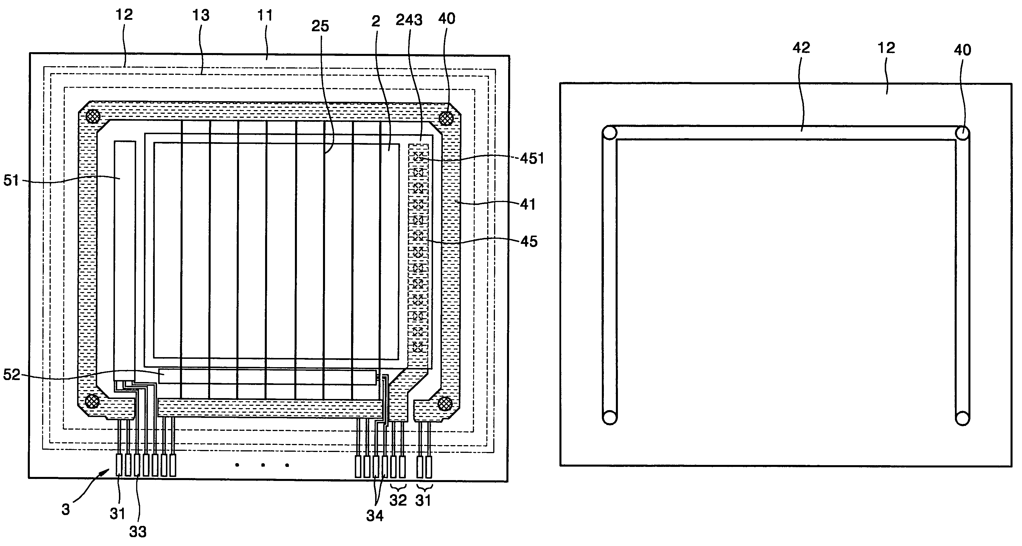
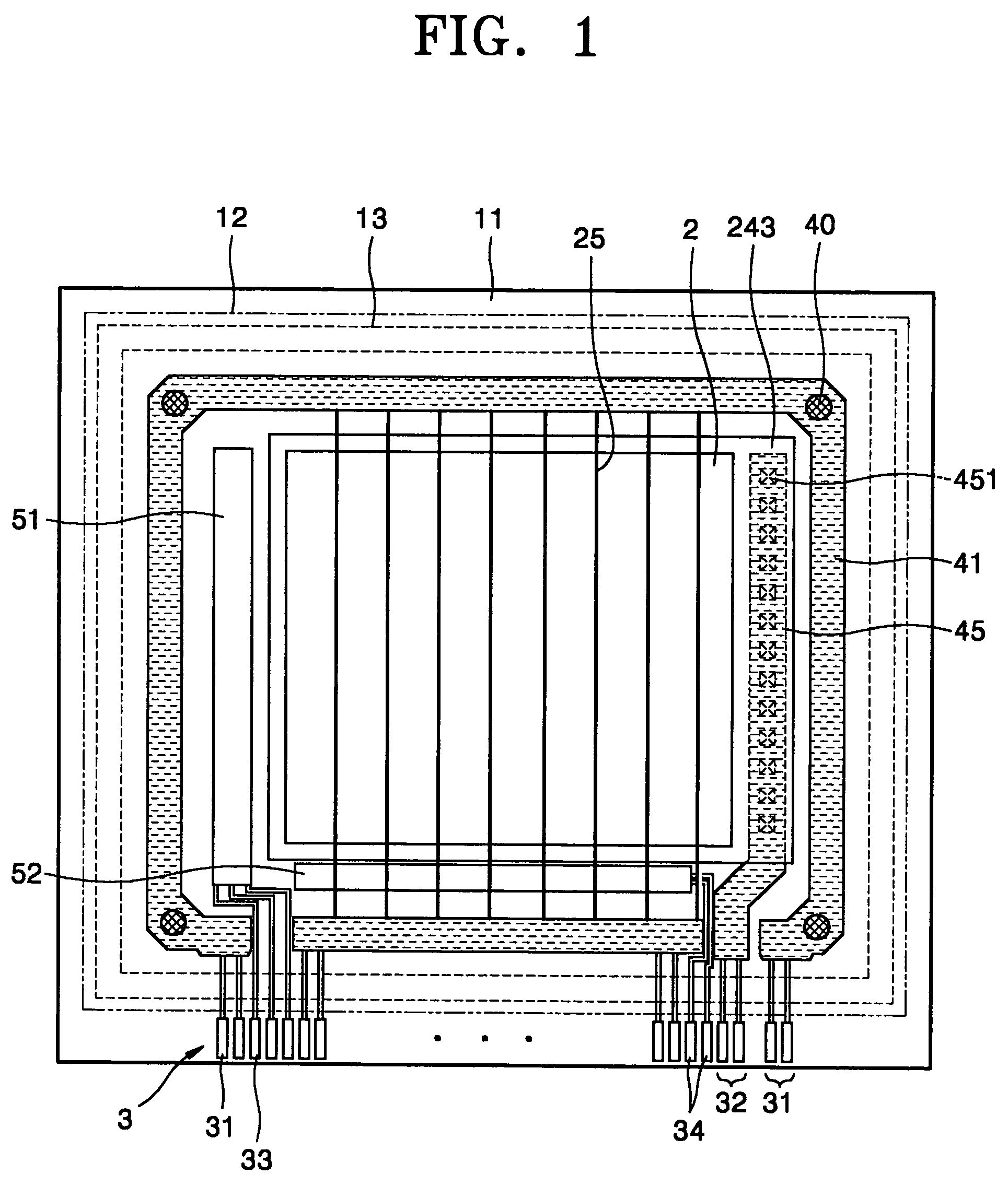
[0022]Referring to FIG. 1, an AM-type EL display comprises a plurality of sub-pixels in a display region 2. Initially, the sub-pixels will be described with reference to FIGS. 7 through 10. However, the present invention is not limited to the structure of the sub-pixels shown in FIGS. 7 through 10.

[0023]FIG. 7 is a partially magnified plan view of four adjacent sub-pixels selected among the sub-pixels of FIG. 1, and FIG. 8 is an equivalent circuit diagram of each of the sub-pixels of FIG. 7.

[0024]Referring to FIG. 8, each of the sub-pixels of the AM-type organic EL display comprises at least two TFTs, of which a first TFT 21 may be for switching and a second TFT 23 may be for driving. The EL display further comprises a capacitor 22, and an organic EL display (hereinafter, referred to as an EL display) 24. A greater number of TFTs and capacitors than the two TFTs and one capacitor illustrated in FIG. 8 may be included, depending on the design specification.

[0025]The first TFT 21 is d...


PUM

PropertyMeasurementUnit
self-luminescentaaaaaaaaaa
conductiveaaaaaaaaaa
luminescentaaaaaaaaaa

Abstract

A flat panel display reduces the line resistance of a driving power supply line and prevents a voltage drop in the driving power supply line so as to obtain uniform resolution and luminance. The flat panel display includes a substrate, a display region formed on the substrate, the display region having a self-luminescent element and VDD lines that supply a driving potential power and / or a source current to the self-luminescent element. Further, a covering member for sealing the display region at least, the covering member being adhered to the substrate to face the substrate and a terminal region formed on one or more edges of the substrate, the terminal region having one or more driving power terminals are provided. In addition, a driving power supply line that connects the driving power terminals to the VDD lines of the display region and a bus conductive unit that is electrically connected to the driving power supply line are provided.

Description

CROSS REFERENCE TO RELATED APPLICATIONS[0001]This application claims the priority of Korean Patent Application No. 2003-54344, filed on Aug. 6, 2003, in the Korean Intellectual Property Office, the disclosure of which is incorporated herein by reference in its entirety.[0002]1. Field of the Invention[0003]The present invention relates to a flat panel display, and more particularly, to a flat panel display with a wide display region.[0004]2. Background of the Invention[0005]Flat panel displays, such as liquid crystal displays (LCDs) or organic or inorganic electro-luminescent (EL) displays, may be categorized as either a passive matrix (PM) type or an active matrix (AM) type, according to the driving method. In a PM type flat panel display, a plurality of anodes and cathodes are arranged in columns and rows, respectively, and a scan signal is transmitted from a row driving circuit to one cathode selected from a row. A data signal is input to each pixel of a column driving circuit.[00...

Claims


Application Information

Patent Timeline
Patent Type & Authority Patents(United States)
IPC IPC(8): H01J1/36G02F1/1345H01L27/12H01L27/32H01L51/52H05B33/00H05B33/06
CPCH01L27/3276H01L27/12H01L51/5237H10K59/131G02F1/1345H10K50/841
Inventor KIM, KUM-NAM
Owner SAMSUNG DISPLAY CO LTD
Learn More