Optical scanning device and method of manufacturing the same

a scanning device and optical technology, applied in the direction of optical elements, mountings, instruments, etc., can solve the problems of limited high-speed scanning technology, low required drive power for rotating the oscillation mirror, and low power consumption, and achieve easy and inexpensive manufacturing. , the effect of small siz

Inactive Publication Date: 2008-07-22
RICOH KK
View PDF20 Cites 9 Cited by
  • Summary
  • Abstract
  • Description
  • Claims
  • Application Information

AI Technical Summary

Benefits of technology

[0015]Accordingly, it is an object of the present invention to provide a sealed optical scanning device mounted on a printed circuit board that is small in size and is easily and inexpensively manufactured without requiring a large number of components and complicated mounting procedures.
[0017]It is another object of the present invention to provide an optical scanning device that is capable of obtaining a large scanning angle by providing a counter mirror facing against the oscillation mirror so that an optical beam is reflected back and forth between the two mirrors.

Problems solved by technology

However, in the prior art, high speed scanning technology is restricted by factors such as the durability of the bearing, heat generation due to windage loss, and noise.
Also, according to this technique, the required drive power for rotating the oscillation mirror is relatively low so that power consumption may be maintained at a low rate.
When an oscillation mirror as is described above is used in an air medium, the following problems arise.
(2) A large scanning angle cannot be obtained due to the viscous resistance of air.
However, complicated processing needs to be conducted using a relatively large number of components including the stem and the cap to realize the above disclosed device structure, and thereby, the manufacturing process for the device structure is quite complicated.
Also, the device structure disclosed in Japanese Laid-Open Patent Publication No. 8-334722 uses an electromagnetic power driven oscillation mirror, and thereby, its manufacturing procedure requires a relatively large number of processes using a relatively large number of components.
Also, it is noted that such a device uses a large number of glass plates so that its manufacturing cost may be increased.

Method used


Image

  • Optical scanning device and method of manufacturing the same
  • Optical scanning device and method of manufacturing the same
  • Optical scanning device and method of manufacturing the same

Examples


Embodiment Construction

[0061]In the following, preferred embodiments of the present invention are described with reference to the accompanying drawings.

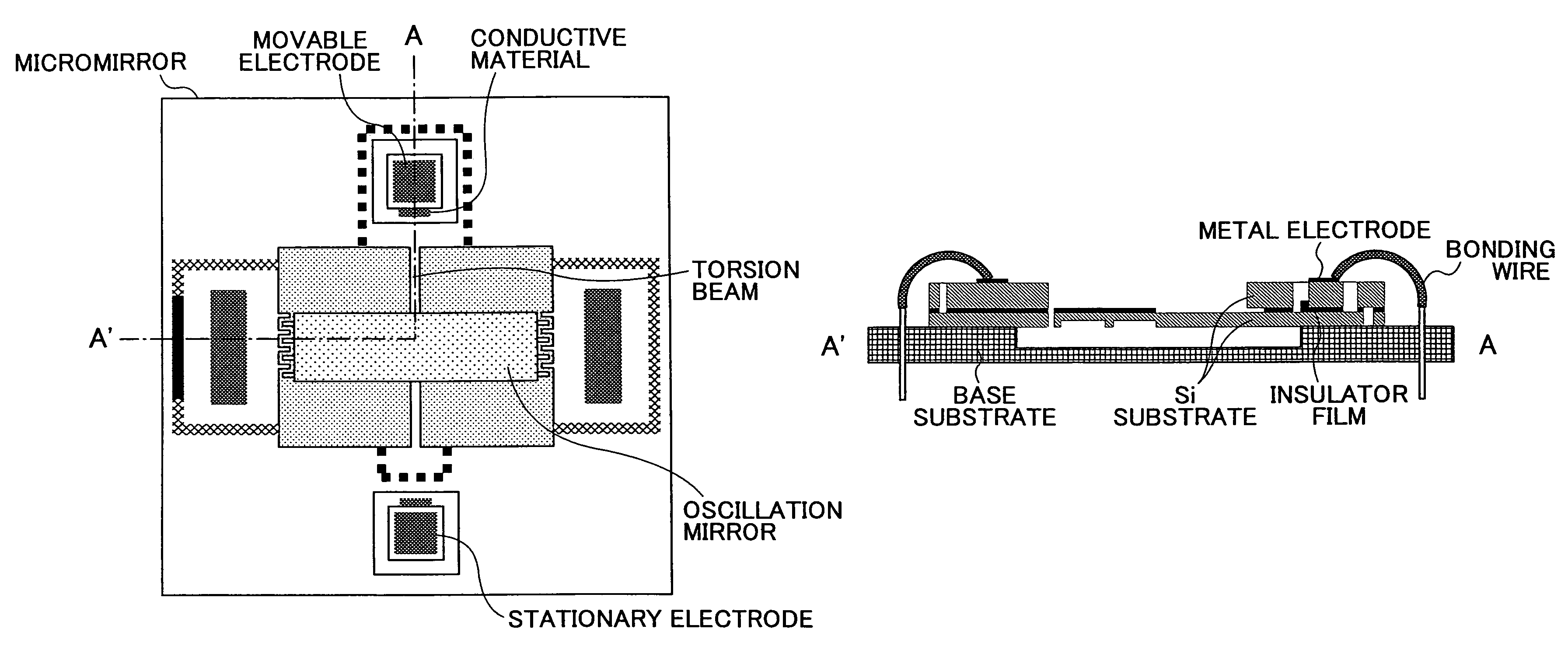
[0062]It is noted that in the embodiments described below, an electrostatic power driven micro mirror is used as an oscillation mirror; however the present invention is not limited to such an embodiment and other types of oscillation mirrors may be used as well.

[0063](Manufacturing Method)

[0064]FIGS. 3A˜3H are diagrams illustrating process steps for manufacturing an optical scanning device in which plural electrodes are aligned in parallel and perpendicular directions. According to the present embodiment, a micro mirror is formed using a SOI (silicon on insulator) substrate. For example, substrates (conductors) with low resistance are used as the substrates of the two sides of the SOI substrate, and an etching process is conducted to form an oscillation space of the oscillation mirror on a thicker one of the substrates and the oscillation mirror on the thi...


PUM


Abstract

An optical scanning device is disclosed that is manufactured through a simple mounting process and is provided with a hermetically sealed oscillation space for an oscillation mirror. The optical scanning device includes plural drive electrodes for driving the oscillation mirror and plural external electrodes of the drive electrodes that are formed at the same height.

Description

BACKGROUND OF THE INVENTION[0001]1. Field of the Invention[0002]The present invention relates to an optical scanning device implementing a movable mirror as a deflector for scanning an optical beam and a method of manufacturing such an optical scanning device.[0003]2. Description of the Related Art[0004]Conventionally, a polygon mirror or a galvanometer mirror is used in an optical scanning device as a deflector for scanning an optical beam. In order to achieve a high resolution image and high-speed printing, the rotational speed of the deflector needs to be increased. However, in the prior art, high speed scanning technology is restricted by factors such as the durability of the bearing, heat generation due to windage loss, and noise.[0005]In response to such a problem, in recent years and continuing, technology is being developed for applying silicon micromachining to an optical deflector. For example, Japanese Patent No. 2924200 and Japanese Patent No. 3022244 disclose technology...

Claims


Application Information

Patent Timeline
Patent Type & Authority Patents(United States)
IPC IPC(8): G02B26/08B41J2/44B81B3/00G02B26/10H04N1/036H04N1/113
CPCG02B26/0841
Inventor MOCHIZUKI, EIJI
Owner RICOH KK
Why Eureka
Try Eureka