Optical switching element

a technology of optical switching elements and switching elements, applied in the field of optical switching elements, can solve the problems of structural fragility of traditional optical switching elements

Inactive Publication Date: 2008-07-22
FUJIFILM BUSINESS INNOVATION CORP
View PDF5 Cites 19 Cited by
  • Summary
  • Abstract
  • Description
  • Claims
  • Application Information

AI Technical Summary

Problems solved by technology

The traditional optical switching elements are structurally fragile since a Y-shaped branching path or an optical path switching coupler is generally used.

Method used


Image

  • Optical switching element
  • Optical switching element
  • Optical switching element

Examples


embodiment

Optical Switching Element

(1) Configuration

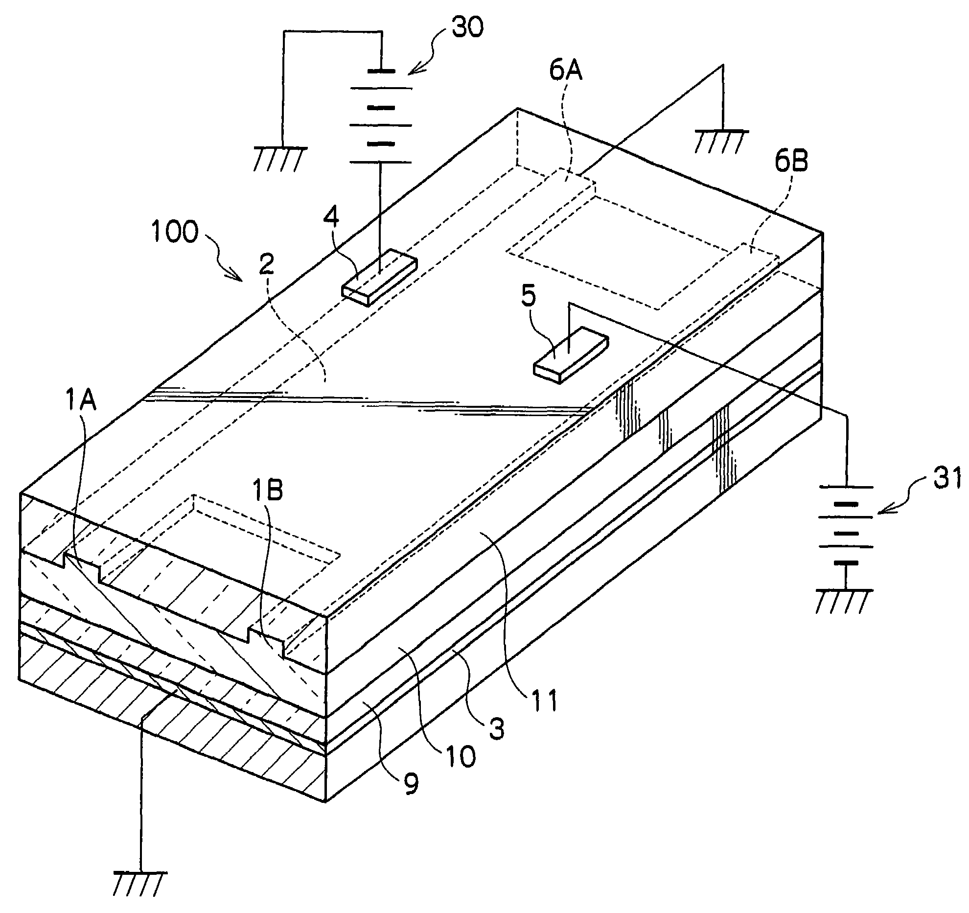
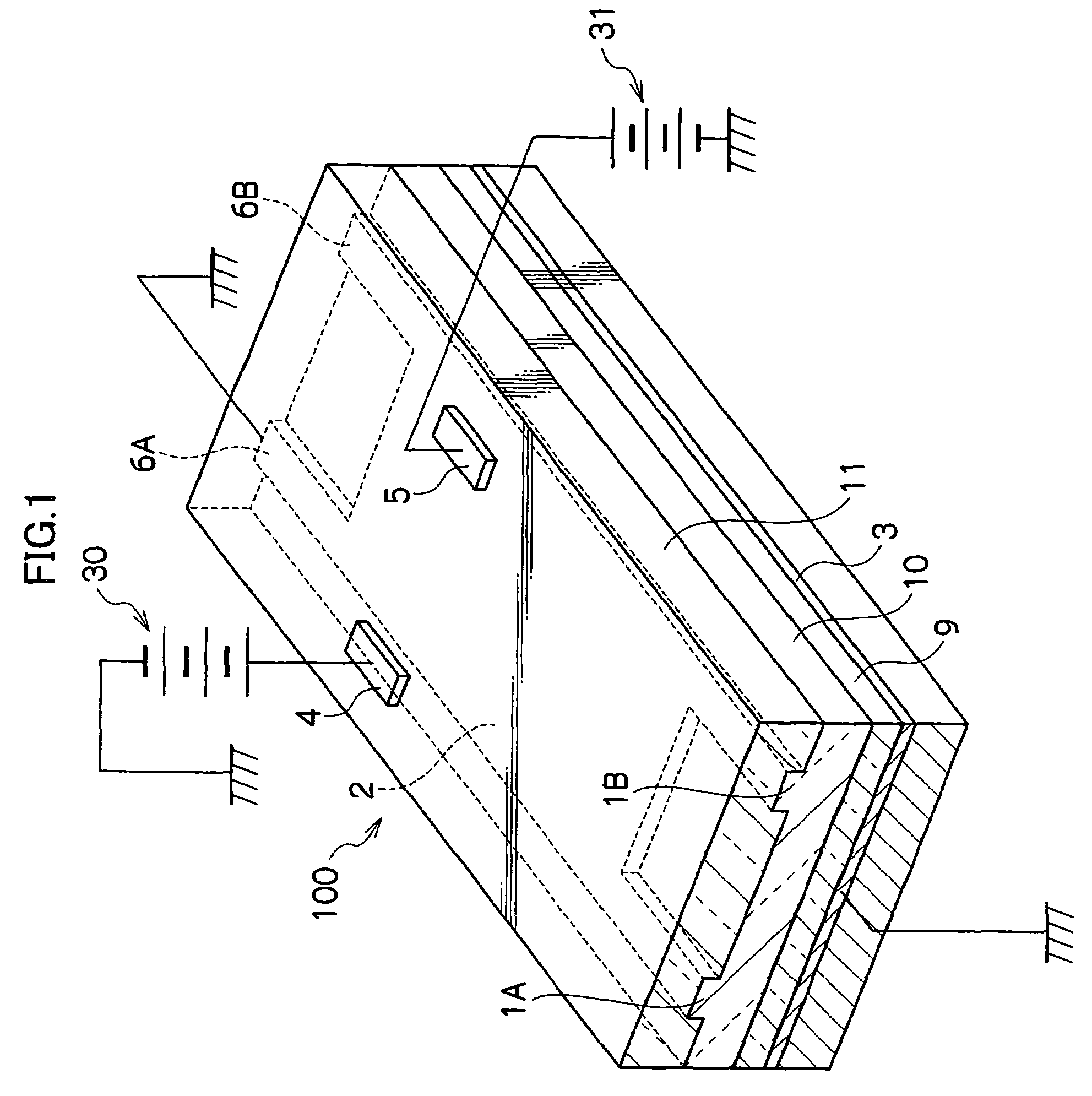
[0038]As shown in FIGS. 1 to 5, an optical switching element 100 according to a first embodiment includes a rectangular multimode waveguide 2; two incident waveguides 1A and 1B (hereinafter collectively referred to sometimes as “incident waveguides 1”) connected to one end of the multimode waveguide 2; two outgoing waveguides 6A and 6B (hereinafter collectively referred to sometimes as “outgoing waveguides 6”) connected to the other end of the multimode waveguide 2; a first electrode 4 and a second electrode 5 arranged above the multimode waveguide 2; and a third electrode 3 arranged below the multimode waveguide 2. The incident waveguides 1A and 1B correspond to a first single mode waveguide in the present invention, and the outgoing waveguides 6A and 6B correspond to a second single mode waveguide in the present invention.

[0039]The incident waveguides 1, the outgoing waveguides 6, and the multimode waveguide 2 are integrally formed with a ...

example

[0079]The optical switching element 100 is formed according to the procedures shown in FIG. 19.

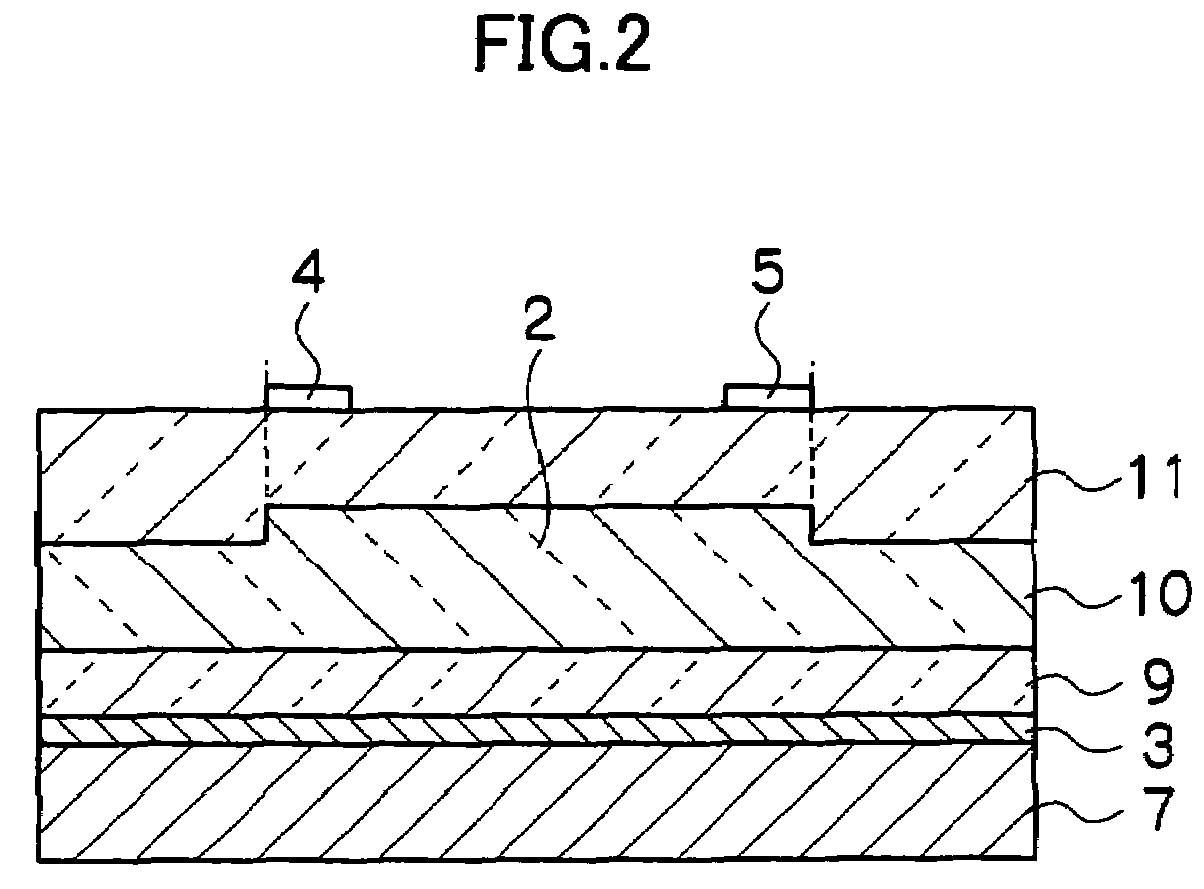
[0080]The third electrode 3 is formed by depositing gold on the substrate 7 through a VCD method. On the third electrode 3, an acrylic resin is spin coated and ultraviolet cured to form the lower cladding layer 9 with a thickness of 3.5 μm.

[0081]The resultant of dispersing Disperse-Red 1 or FTC (2-dicyanomethylene-3-cyano-4-{2-[trans-(4-N,N-diacetoxyethyl-amino)phenylene-3,4-dibutylene-5]vinyl}-5,5-dimethyl-2,5-dihydrofuran) in amorphous polycarbonate is spin coated onto the lower cladding layer 9, and then heating and curing are performed to form the core layer 10 with a thickness of 3.2 μm.

[0082]Subsequently, the incident waveguides 1A and 1B; the multimode waveguide 2; and the outgoing waveguides 6A and 6B are formed by etching the core layer. The width W1 of the incident waveguides 1 and the outgoing waveguides 6 is 5 μm, and the width W2 of the multimode waveguide 2 is 50 μm. Therefor...


PUM

PropertyMeasurementUnit
refractive index n1aaaaaaaaaa
refractive indexaaaaaaaaaa
voltageaaaaaaaaaa

Abstract

An optical switching element comprising: a multimode waveguide having an electro-optical effect; one or a plurality of first single mode waveguides; a plurality of second single mode waveguides; a first electrode arranged in the vicinity of one edge on one side of the multimode waveguide; a second electrode arranged in the vicinity of the other edge on the same side of the multimode waveguide; and a third electrode arranged on the other side of the multimode waveguide, over the first electrode and the second electrode being arranged so as to be positioned on bright spots formed by multimode interference in an optical mode field generated by the light propagating through the multimode waveguide, and an optical path being switched between the first single mode waveguide and the second single mode waveguide by applying voltage between the first electrode and the third electrode and between the second electrode and the third electrode, is provided.

Description

BACKGROUND[0001]1. Technical Field[0002]The present invention relates to optical switching elements, more specifically, to an optical switching element capable of switching an optical path at low operating voltage.[0003]2. Related Art[0004]The optical switching element having a rigid structure and operating at high speed at low operating voltage is required to build the next generation of optical data links. The traditional optical switching elements are structurally fragile since a Y-shaped branching path or an optical path switching coupler is generally used.[0005]On the other hand, a multimode interference (MMI) that utilizes the interference of light is robust to unintentional alteration in refractive index and assembly failure and is a promising technology for the future, but traditionally, MMIs have only been used as passive elements in optical switching elements.SUMMARY[0006]According to an aspect of the present invention, there is provided: an optical switching element compr...

Claims


Application Information

Patent Timeline
Patent Type & Authority Patents(United States)
IPC IPC(8): G02B6/42G02B6/10G02F1/295
CPCG02F1/3132G02F2202/07G02F2001/217G02F1/3136G02F1/217
Inventor THAPLIYA, ROSHANNAKAMURA, SHIGETOSHIKIKUCHI, TAKASHI
Owner FUJIFILM BUSINESS INNOVATION CORP
Why Eureka
Try Eureka