InP-based wavelength division-mode division multiplexing few-mode communication photon integrated emission chip

A mode division multiplexing and photonic integration technology, applied in the directions of light guides, optics, optical components, etc., to achieve the effect of large optical bandwidth, small size, large design and process tolerance

Active Publication Date: 2015-11-18
INST OF SEMICONDUCTORS - CHINESE ACAD OF SCI
View PDF5 Cites 14 Cited by
  • Summary
  • Abstract
  • Description
  • Claims
  • Application Information

AI Technical Summary

Problems solved by technology

Due to the limitation of Shannon limit, the current limit of communication network based on single-...

Method used


Image

  • InP-based wavelength division-mode division multiplexing few-mode communication photon integrated emission chip
  • InP-based wavelength division-mode division multiplexing few-mode communication photon integrated emission chip
  • InP-based wavelength division-mode division multiplexing few-mode communication photon integrated emission chip

Examples


Embodiment Construction

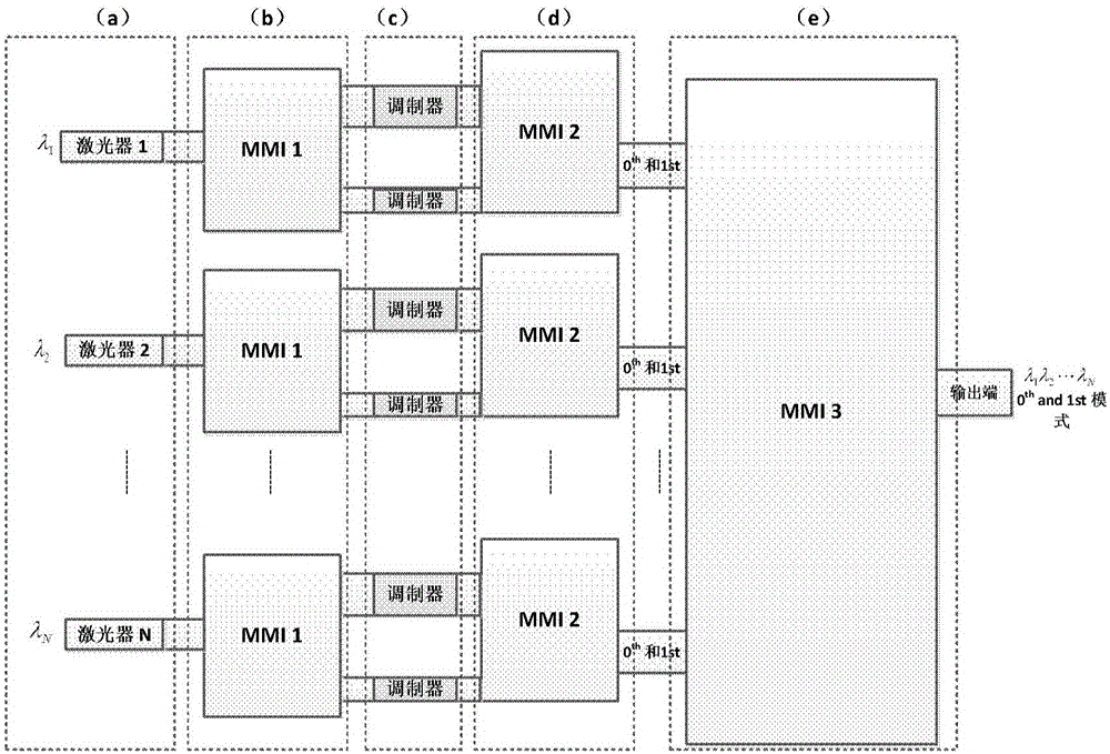
[0027] The present invention proposes an InP fundamental wavelength division-mode division multiplexing few-mode optical communication photon integrated emission chip, and its working structure and principle are as follows:

[0028] The overall design of the transmitter chip is as figure 1 shown, where figure 1 (a) is a single-mode semiconductor laser part, figure 1 (b) is the beam splitter part based on MMI, figure 1 (c) is the modulator part, figure 1 (d) is the MMI-based mode converter and mode multiplexer part, figure 1 (e) is the focus of the design of the present invention, that is, an MMI-based multi-wavelength multi-mode coupler.

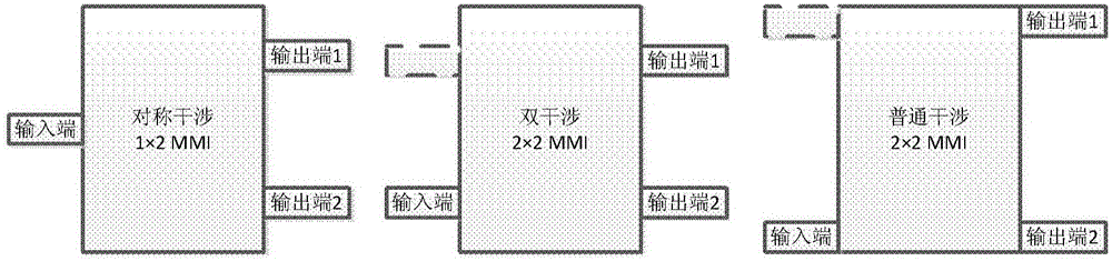
[0029] Semiconductor laser Laser1 generates light in the fundamental transverse mode of the single longitudinal mode, which enters MMI1 through a passive waveguide. The schematic diagram of MMI1 is shown in figure 2 As shown in , at this time, MMI1 will divide the input light into two paths and load the modulated signal through the mod...


PUM


Abstract

An InP-based wavelength division-mode division multiplexing few-mode communication photon integrated emission chip includes: multiple single-mode semiconductor lasers with different wavelengths, the semiconductor lasers serving as light sources; multiple multimode interference couplers (MMI) having different functions and used for optical power distribution, mode conversion and multi-wavelength multimode multiplexing; and multiple modulator structures for modulation of basic mode signals. The above parts are connected through straight waveguides or bent waveguides. The excellent characteristics of the multiple multimode interference couplers are that the couplers exhibit great design and technical tolerance, have great optical bandwidth, are insensitive to polarization, are small in size, etc. The multimode interference couplers are utilized to serve as multi-wavelength multimode couplers for the first time, wavelength division multiplexing and mode division multiplexing are combined, and thus the fiber transmission capacity is further improved.

Description

technical field [0001] The present application relates to the technical field of few-mode optical communication, and in particular to an InP fundamental wavelength division-mode division multiplexing few-mode optical communication photonic integrated launch chip, which is mainly used in long-distance trunk few-mode optical fiber communication systems. Background technique [0002] With the development of optical fiber communication technology, the requirements for transmission capacity are getting higher and higher. In the past ten years, the demand for transmission capacity has increased by 100 times, which makes the current optical communication transmission technology face a huge challenge. Due to the limitation of Shannon's limit, the current limit of the communication network based on single-mode transmission is 100Tb / s, and this transmission capacity limit has also been confirmed by experiments. According to the current demand for the growth of optical communication tr...

Claims


Application Information

Patent Timeline
IPC IPC(8): G02B6/293
CPCG02B6/29346G02B6/2938
Inventor 李召松陆丹张莉萌余力强戴兴潘教青
Owner INST OF SEMICONDUCTORS - CHINESE ACAD OF SCI
Why Eureka
Try Eureka