Multimode interference waveguide type optical switch

a waveguide and optical switch technology, applied in the field of multimode interference waveguide optical switch, can solve the problems of increasing the electric power needed, increasing the switching time, and increasing the capacitan

Inactive Publication Date: 2010-12-28
KEIO UNIV
View PDF32 Cites 14 Cited by
  • Summary
  • Abstract
  • Description
  • Claims
  • Application Information

AI Technical Summary

Benefits of technology

[0053]Effects achieved by the typical aspects of the invention disclosed by this patent application are briefly described as follows.
[0054](1) A low-electric-power, high-speed switch can be provided by reducing the area of an electrode.
[0055](2) A digital optical switch that is high in extinction ratio and that is low in crosstalk can be structured by allowing a total reflection surface to have a symmetric structure.
[0056](3) A basic design to make the optical switch compact is disclosed.
[0057](4) To reducing a driving voltage, the structure that uses a tapered waveguide by which a higher mode in a multimode interference waveguide is decreased is disclosed.
[0058](5) It becomes possible to structure an optical switch that uses the plasma effect in a semiconductor or the electro-optic effect of, for example, PLZT in which the refractive index is decreased by injecting current.

Problems solved by technology

The problem of this structure is that it is necessary to vary the refractive index all over the area in which light is guided and that the widened area of the electrode causes an increase of electric power necessary for switching and causes an increase in switching time resulting from an increase in capacitance.
Additionally, although this conventional technique uses the method of increasing the refractive index of a part disposed under the electrode, the plasma effect by injecting current into the semiconductor and the electro-optic effect of material, such as PLZT (lanthanum-doped lead zirconate titanate), cannot be used in the structure of this conventional technique, because the refractive index is decreased by injecting current or applying voltage.
Therefore, it is difficult to improve the crosstalk and extinction ratio characteristics.
In other words, a problem resides in the fact that a switching voltage becomes high.
Additionally, no consideration is given to the fact that the area of the electrode is large, and hence electric power necessary for switching is increased, and an increase in switching time resulting from an increase in capacitance is caused.

Method used


Image

  • Multimode interference waveguide type optical switch
  • Multimode interference waveguide type optical switch
  • Multimode interference waveguide type optical switch

Examples


embodiment 1

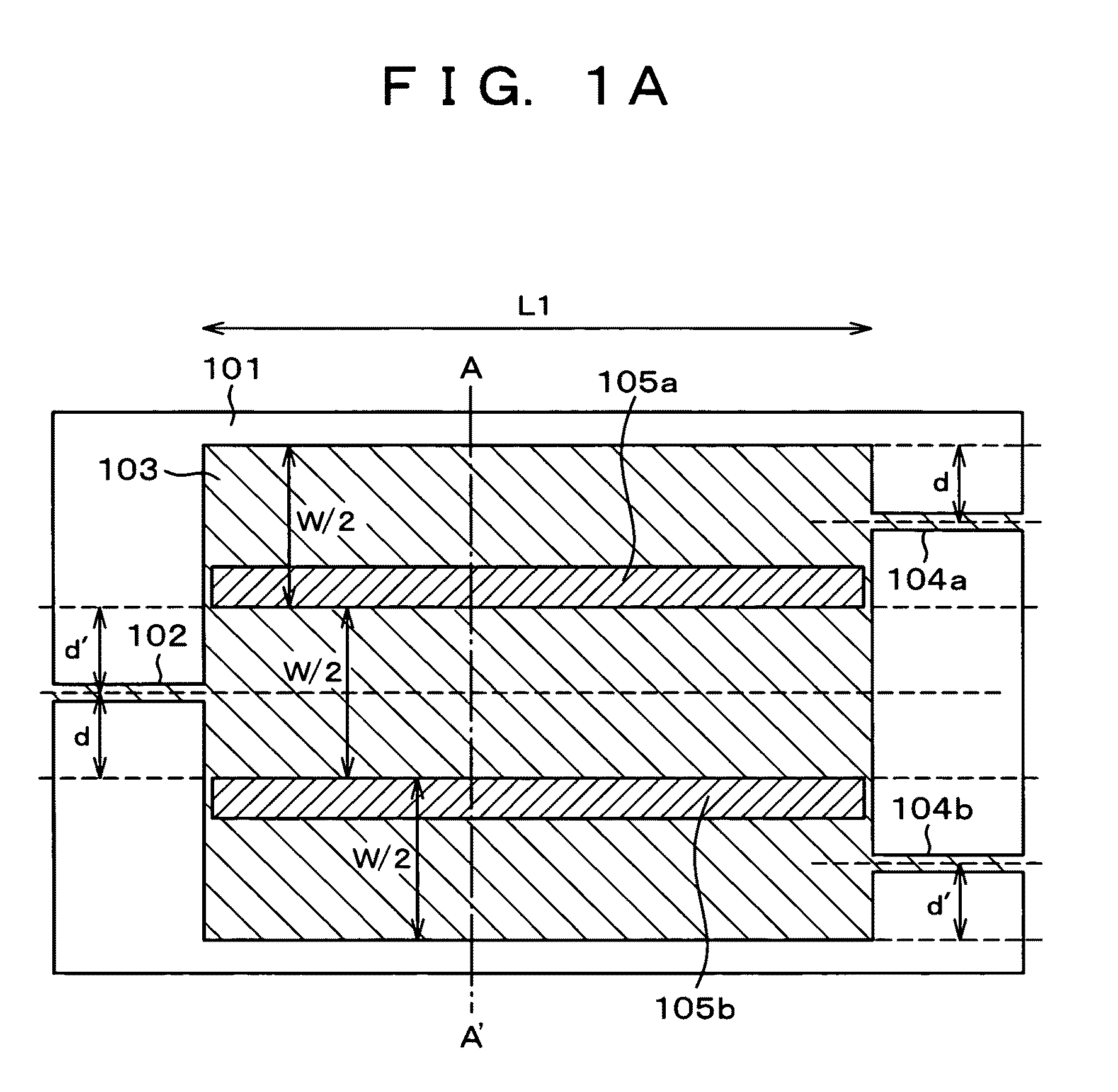
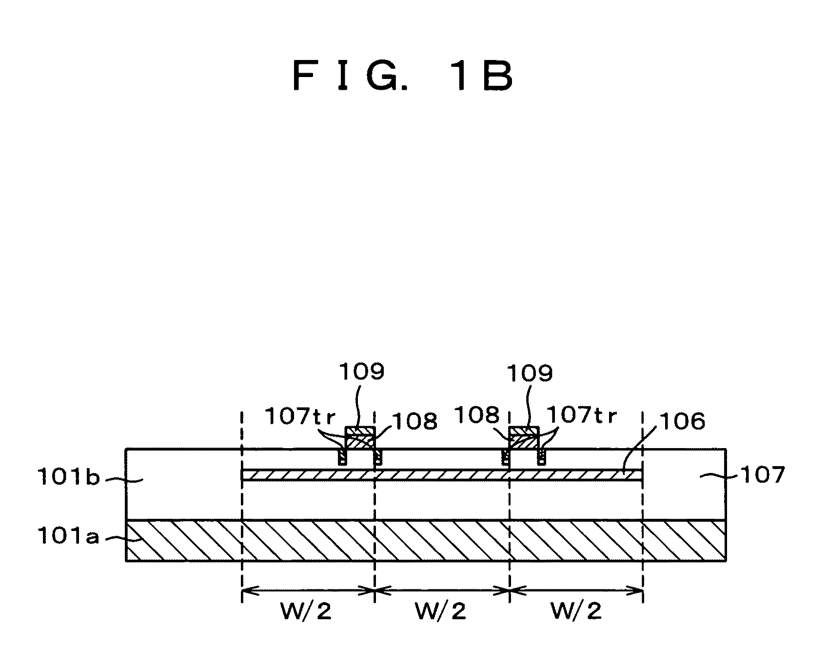
[0151]A first embodiment is shown in FIG. 1A. In FIG. 1A, reference sign 101 designates an optical waveguide substrate, reference sign 102 designates an input waveguide (input single-mode waveguide), reference sign 103 designates a multimode interference waveguide, reference signs 104a and 104b designate output waveguides (output single-mode waveguides), and reference signs 105a and 105b designate electrodes. FIG. 1B shows a cross section along line A-A′ of FIG. 1A. In this embodiment, the structure of the waveguide is that of a PLZT waveguide. However, the material system is not limited to PLZT. In FIG. 1B, reference sign 101a designates a semiconductor niobium-doped strontium titanate substrate, reference sign 101b designates a waveguide layer which consists of a PLZT core 106 and a PLZT cladding 107, reference sign 108 designates an ITO (Indium Tin Oxide) electrode, and reference sign 109 designates a gold electrode. Reference sign 107tr designates a separation groove formed so t...

embodiment 2

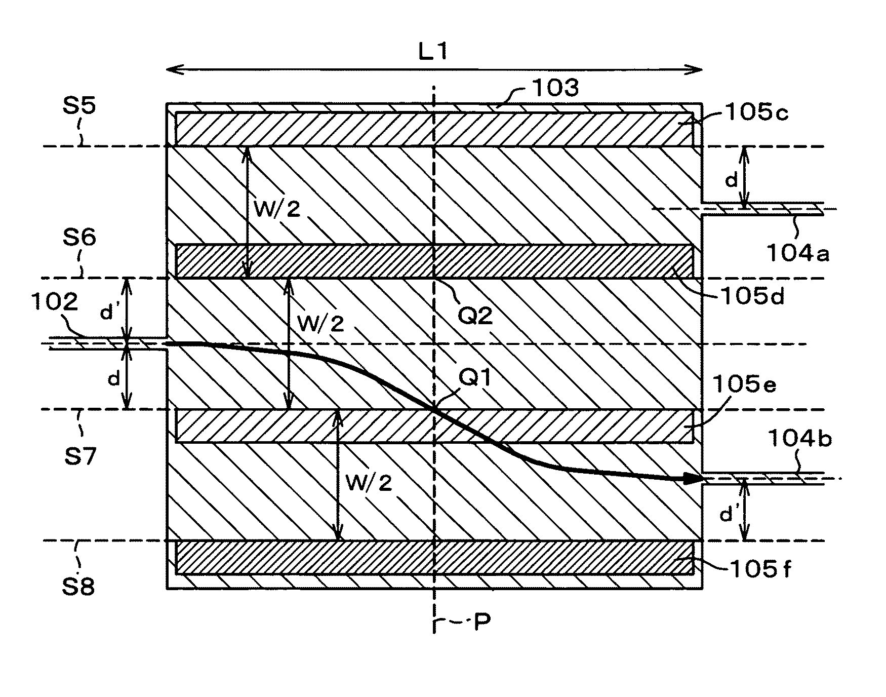
[0156]A second embodiment is shown in FIG. 2A and FIG. 2B. This embodiment differs from the first embodiment in that the number of upper surface electrodes for controlling the refractive index is increased to have four electrodes (105c to 105f). In the first embodiment, the places that function as total reflection side surfaces are one side where a refractive index difference occurs by applying a voltage, whereas the other side is a part having a refractive index difference provided by a waveguide structure. These are not the same in structure, and are asymmetrical. However, in this second embodiment, both of the total reflection side surfaces are created by a refractive-index variation resulting from the application of a voltage, and have a completely symmetrical structure. When a voltage is applied to the electrodes 105d and 105f, the broken line S6 and the broken line S8 serve as a total reflection side surface of the multimode interference waveguide. Light entered from the input...

embodiment 3

[0157]A third embodiment is shown in FIG. 3A to FIG. 3C. This embodiment has a switch structure capable of simultaneous switching among a plurality of inputs. Although the switching mechanism is the same as in the second embodiment, the broken line S6 and the broken line S8 serve as a total reflection side surface of the multimode interference waveguide when a voltage is applied to the electrodes 105d and 105f. Light entered from the input waveguides 110a and 110b is imaged at a position symmetrical with respect to an intersection Q1 of the broken line S7 and the broken line P by which a rectangular waveguide is halved, i.e., at the position of the output waveguides 111b and 111a, and is output. Additionally, the broken line S5 and the broken line S7 serve as a total reflection side surface of the multimode interference waveguide when a voltage is applied to the electrodes 105c and 105e. Light entered from the input waveguides 110a and 110b is imaged at a position symmetrical with r...


PUM


Abstract

It is an object of the present invention to provide a multimode interference waveguide type optical switch that has a wide tolerance and that digitally performs switching with respect to a change in an applied voltage or injected current. The multimode interference waveguide type optical switch of the present invention includes an input single-mode waveguide (102) into which input light is entered, a multimode rectangular slab waveguide (103) into which light emitted from the input single-mode waveguide is entered, two electrodes (105a, 105b) that are arranged in parallel in a waveguide direction on the slab waveguide and that decrease the refractive index of the slab waveguide (103) disposed thereunder by injecting current or applying voltage, and a plurality of output single-mode waveguides (104a, 104b) into which light emitted from the slab waveguide (103) is entered and from which output light is emitted.

Description

TECHNICAL FIELD[0001]The present invention relates to a multimode interference waveguide type optical switch suitable to be applied to a switching processing circuit in an optical communication network node.BACKGROUND ART[0002]FIG. 13 and FIG. 14 show conventional, typical optical switch structures each of which uses a multimode slab waveguide. These structures are disclosed by Patent Document 1 titled “Optical Switch” and Patent Document 2 titled “Multimode Interference Waveguide Type Optical Switch,” respectively.[0003]In the structure of FIG. 13, two parallel electrodes are arranged on a multimode interference device, and a switching operation is performed to modulate the refractive index of a waveguide disposed under the electrodes by applying voltage or by injecting current to the electrodes. Reference sign 201 designates a multimode interference waveguide, which consists of two parts 202a and 202b. Reference sign 203 designates an input waveguide. Reference sign 204 designates...

Claims


Application Information

Patent Timeline
Patent Type & Authority Patents(United States)
IPC IPC(8): G02B6/26G02B6/42
CPCG02F1/3132G02B6/2813G02B6/354
Inventor TSUDA, HIROYUKIYASUMOTO, MITSUHIRO
Owner KEIO UNIV
Why Eureka
Try Eureka