Semiconductor device containing stacked semiconductor chips and manufacturing method thereof

a semiconductor chip and semiconductor technology, applied in the direction of conductive pattern reinforcement, printed circuit aspects, metal adhesion improvement of insulation substrates, etc., can solve the problems of reducing connection strength, affecting the resistance and connection strength at the connecting point, and changing the surface property of pad electrodes, so as to improve the formation of mold resin and dielectric films. , the effect of suppressing the degradation of the surface of the pad electrod

Inactive Publication Date: 2008-07-29
SANYO ELECTRIC CO LTD
View PDF16 Cites 98 Cited by
  • Summary
  • Abstract
  • Description
  • Claims
  • Application Information

AI Technical Summary

Benefits of technology

[0010]The present invention is achieved in view of the aforementioned circumstances and an object thereof is to provide a technique capable of suppressing bad connection between a semiconductor chip and an interconnect layer so that element reliability and a yield rate are improved.
[0014]According to the present invention, degradation of surface of pad electrodes can be suppressed since a conductive protective film is provided on the surface of the pad electrodes.
[0016]The semiconductor device may have a construction in which the dielectric film has a concave part, the pad electrode is formed inside the concave part, and a void part is provided between the inside wall of the concave part and the side wall of the pad electrode. With this construction, the adhesion for the film, such as mold resin, formed on the dielectric film can be improved. Furthermore, the surface of the pad electrode becomes less subject to the attachment of particles of the dielectric film material.

Problems solved by technology

The resistance and the connection strength at the connecting point are not obtained enough in some package formation processes.
As a result, they found that the surface property of pad electrodes was changed so that the connection strength declines, when a process such as a plasma treatment, which changes a property of metal surface, is implemented in an element mounting process on the interconnect layer.

Method used


Image

  • Semiconductor device containing stacked semiconductor chips and manufacturing method thereof
  • Semiconductor device containing stacked semiconductor chips and manufacturing method thereof
  • Semiconductor device containing stacked semiconductor chips and manufacturing method thereof

Examples


Embodiment Construction

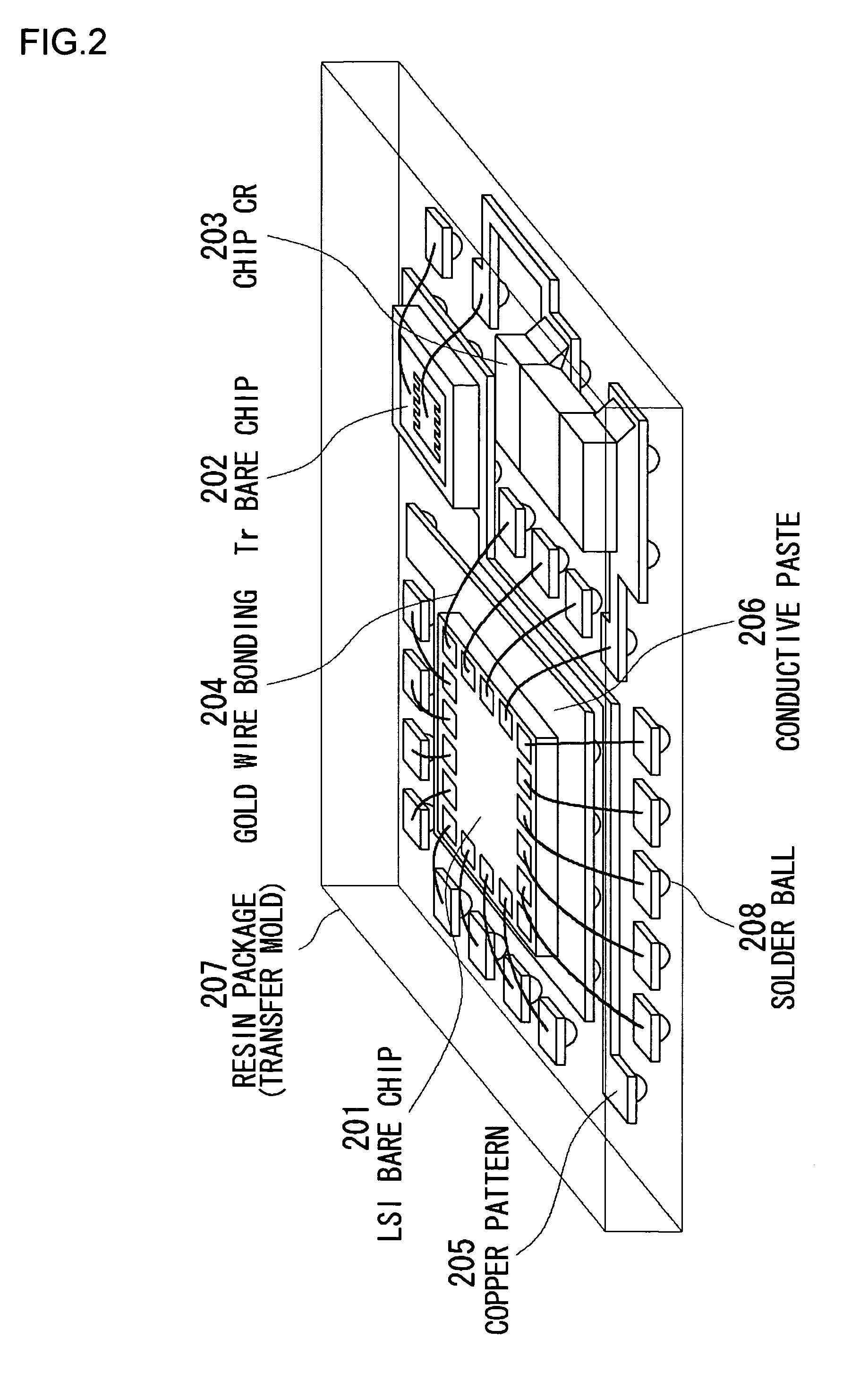
[0032]Although the invention will be described below based on the preferred embodiments, the ISB™ configuration introduced in each embodiment will be now described prior to it. ISB™ (Integrated System in Board) is a unique package developed by the inventors of the present invention. ISB™ is a unique coreless system-in package in the packaging techniques involving electric circuits including semiconductor bare chips mainly, and it has interconnect patterns made of copper but no core (base material) to support circuit components.

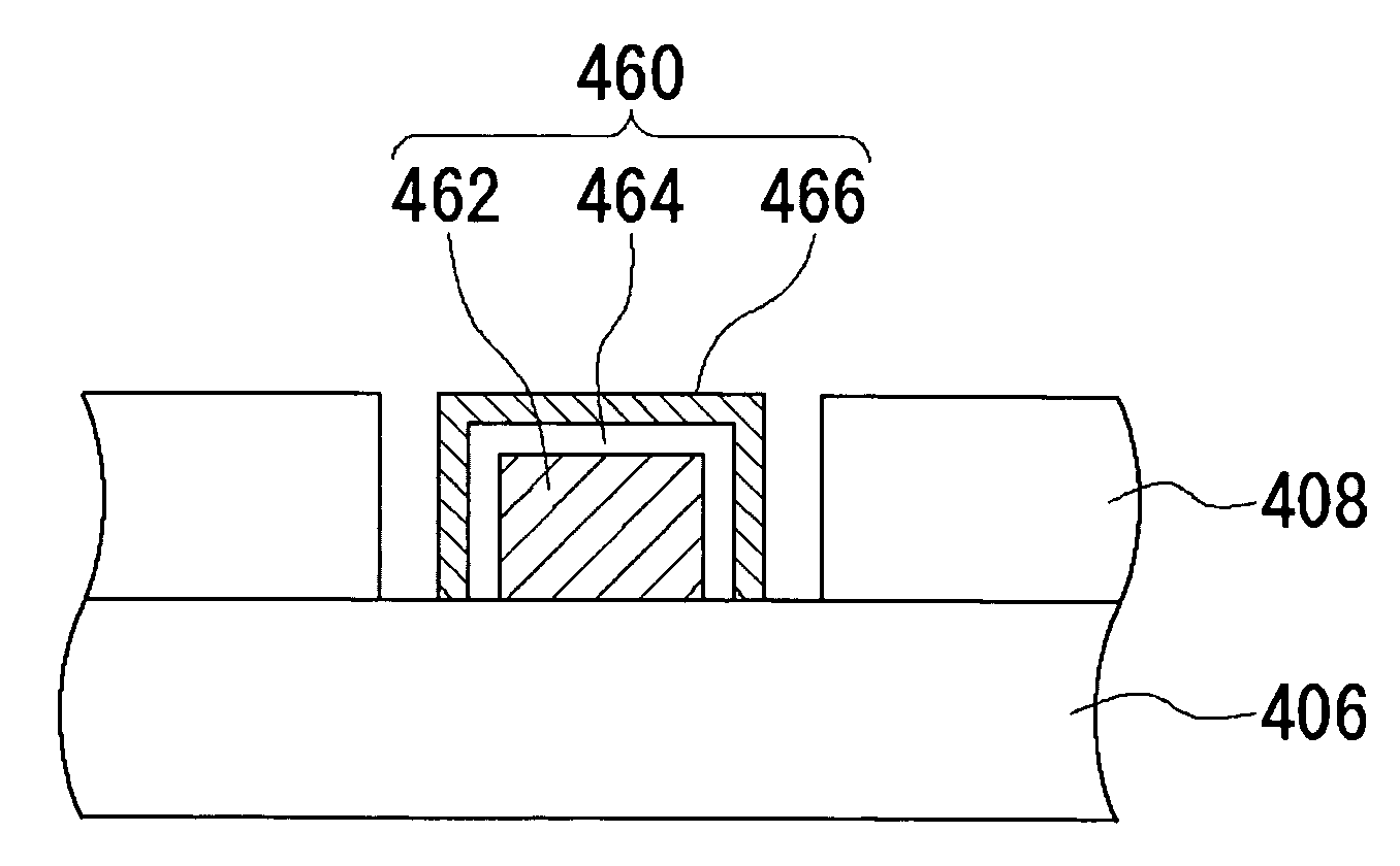
[0033]FIG. 2 shows a schematic illustration of an example of ISB™. Although a single interconnect layer is shown for a simple explanation of the overall configuration of ISB™, the configuration practically includes a plurality of interconnect layers stacked. This ISB™ has a configuration that includes the LSI bare chip 201, Tr bare chip 202 and the chip CR 203 connected by interconnect lines that include the copper pattern 205. The LSI bare chip 201 is connect...


PUM

PropertyMeasurementUnit
thicknessaaaaaaaaaa
diameteraaaaaaaaaa
diameteraaaaaaaaaa

Abstract

An adhesive film is formed on an electrode film, and a coating film is formed thereon. Nickel, chrome, molybdenum, tungsten, aluminum or an alloy of them is used as a constituent material of the adhesive film. Gold, silver, platinum or an alloy of them is used as a constituent material of the coating film.

Description

BACKGROUND OF THE INVENTION[0001]1. Field of the Invention[0002]This invention relates to a semiconductor device provided with semiconductor chips, and a manufacturing method thereof.[0003]2. Description of the Related Art[0004]Portable electronics devices such as a cellular phone, a PDA, a DVC and a DSC become increasingly sophisticated. The fabrication of the devices with a compact size and lightweight are indispensable so that such devices are accepted in the market. System LSI higher integrated is required for the realization of such devices. On the other hand, LSI used for the devices is required to be with a high functionality and a high performance for the realization of friendly and convenient electronics devices. For this reason, while the number of I / O is. increasing with the acceleration of LSI chip integration, downsizing of the package is also required. The development of the packages appropriate to the board assembly of semiconductor components with a high density is s...

Claims


Application Information

Patent Timeline
Patent Type & Authority Patents(United States)
IPC IPC(8): H01L23/48H01L23/12H01L21/68H01L23/31H01L23/498H01L25/16H05K3/24H05K3/30H05K3/34H05K3/38
CPCH01L21/6835H01L23/498H01L25/16H05K3/244H01L23/3128H01L2924/13055Y10S438/906H01L2924/01028H01L2924/01013H01L24/48H01L24/45H01L2221/68345H01L2224/45144H01L2224/48091H01L2224/48227H01L2924/01004H01L2924/01029H01L2924/0105H01L2924/01078H01L2924/01079H01L2924/14H01L2924/15311H01L2924/19041H01L2924/19105H05K3/305H05K3/3452H05K3/381H05K2201/0989H05K2203/049H05K2203/095H01L2924/00014H01L2924/00H01L2924/12042H01L2924/181H01L2224/73265H01L24/49H01L2224/05554H01L2224/49175H01L2224/0603H01L2224/49171H01L2924/00012H01L23/12
Inventor USUI, RYOSUKEMIZUHARA, HIDEKINAKAMURA, TAKESHI
Owner SANYO ELECTRIC CO LTD
Why Eureka
Try Eureka