Techniques for capturing signals at output pins in a programmable logic integrated circuit

a technology of programmable logic and output pins, applied in the field of programmable logic integrated circuits, can solve the problems of inability of the receiving chip to capture interconnect test signals applied to the output pins, failure of jtag sample instruction, and inability to work properly, etc., to achieve the effect of less time and easy implementation

Inactive Publication Date: 2008-07-29
ALTERA CORP
View PDF10 Cites 24 Cited by
  • Summary
  • Abstract
  • Description
  • Claims
  • Application Information

AI Technical Summary

Benefits of technology

[0011]The logic gates enable the input buffer so that the input buffer can capture a test signal at the output pin. The output buffer coupled to the pin that receives the test signal is tristated to prevent contention during the JTAG sampling phase. Th...

Problems solved by technology

If one of the receiving chips does not capture the correct test signal value, the interconnect lines are not functioning properly, possibly because of an open circuit or short circuit on one of the interconnect lines.
Because the input buffers for the programmed output pins are turned off, the receiving chip cannot capture interconnect test signals applied to the output pins during the JTAG test phase.
As a result, the JTAG sample instruction f...

Method used


Image

  • Techniques for capturing signals at output pins in a programmable logic integrated circuit
  • Techniques for capturing signals at output pins in a programmable logic integrated circuit
  • Techniques for capturing signals at output pins in a programmable logic integrated circuit

Examples


Embodiment Construction

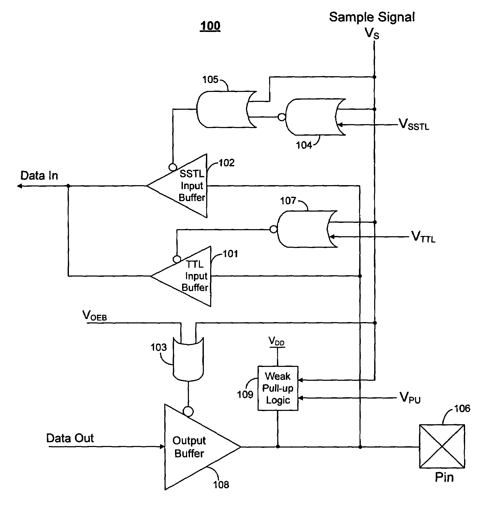
[0017]FIG. 1 illustrates a portion 100 of an input / output (IO) block on a programmable logic integrated circuit chip, such as a field programmable gate array (FPGA), a programmable logic device, or a mask FPGA / PLD.

[0018]IO portion 100 of the chip is designed to receive a signal at pin 106 that is used to test external resources such as board level interconnects according to an embodiment of the present invention. The present invention can be used to test a variety of interconnections. For example, IO portion 100 can receive a signal that indicates the operability of a board level interconnect line that routes signals between two IC chips.

[0019]Board level interconnects are tested during a JTAG sampling phase of a boundary scan according to the IEEE JTAG 1149.1 standard. During the JTAG sampling phase, a signal is driven to a receiving chip to test the operability of the board level interconnect. A JTAG sample signal VS is high during the JTAG sampling phase. Pin 106 is programme...


PUM


Abstract

Techniques are provided for capturing external signals at output pins on a programmable logic integrated circuit (IC) during a boundary scan test. A JTAG sample signal is routed to an input/output block on a chip and active during a JTAG sampling phase. An input buffer coupled to an output pin is turned on during the JTAG sample phase. Logic gates enable the input buffer in response to the JTAG sample signal so that the input buffer can capture a signal on the pin. The input buffer is turned off after the JTAG sampling phase to conserve power. The output buffer coupled to the pin that receives the test signal is tristated to prevent contention during the JTAG sampling phase. The techniques of the present invention can be used to test board level interconnects in less time and are easy to implement.

Description

BACKGROUND OF THE INVENTION[0001]1. Field of the Invention[0002]The present invention relates to programmable logic integrated circuits, and more particularly, to techniques for capturing signals at output pins in a programmable logic integrated circuit.[0003]2. Description of Related Art[0004]Often referred to as the JTAG standard after the Joint Test Action Group that developed it, the JTAG standard provides boundary-scan testing and debugging of printed circuit boards (PCBs) and systems to solve physical access problems on PCBs caused by crowded assemblies. The JTAG standard also provides in-system programming (ISP) of flash memory and field programmable gate arrays (FPGAs).[0005]Boundary scan is a methodology that allows the control and observation of the boundary pins of a JTAG compatible device via software control. Boundary scan provides in-circuit testing without in-circuit test equipment. Boundary-scan testing embeds test circuitry at the chip level to form a complete board...

Claims


Application Information

Patent Timeline
IPC IPC(8): G01R31/28
CPCG01R31/31715G01R31/318516H04L25/0292H04L25/028G01R31/318533
Inventor LAU, KER YON
Owner ALTERA CORP
Why Eureka
Try Eureka