

Master-slave flip-flop and clocking scheme
- Summary
- Abstract
- Description
- Claims
- Application Information
AI Technical Summary
Benefits of technology
Problems solved by technology
Method used
Image

Examples
Embodiment Construction
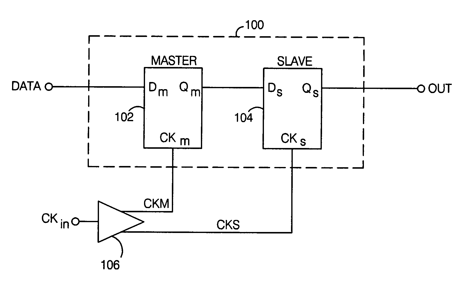
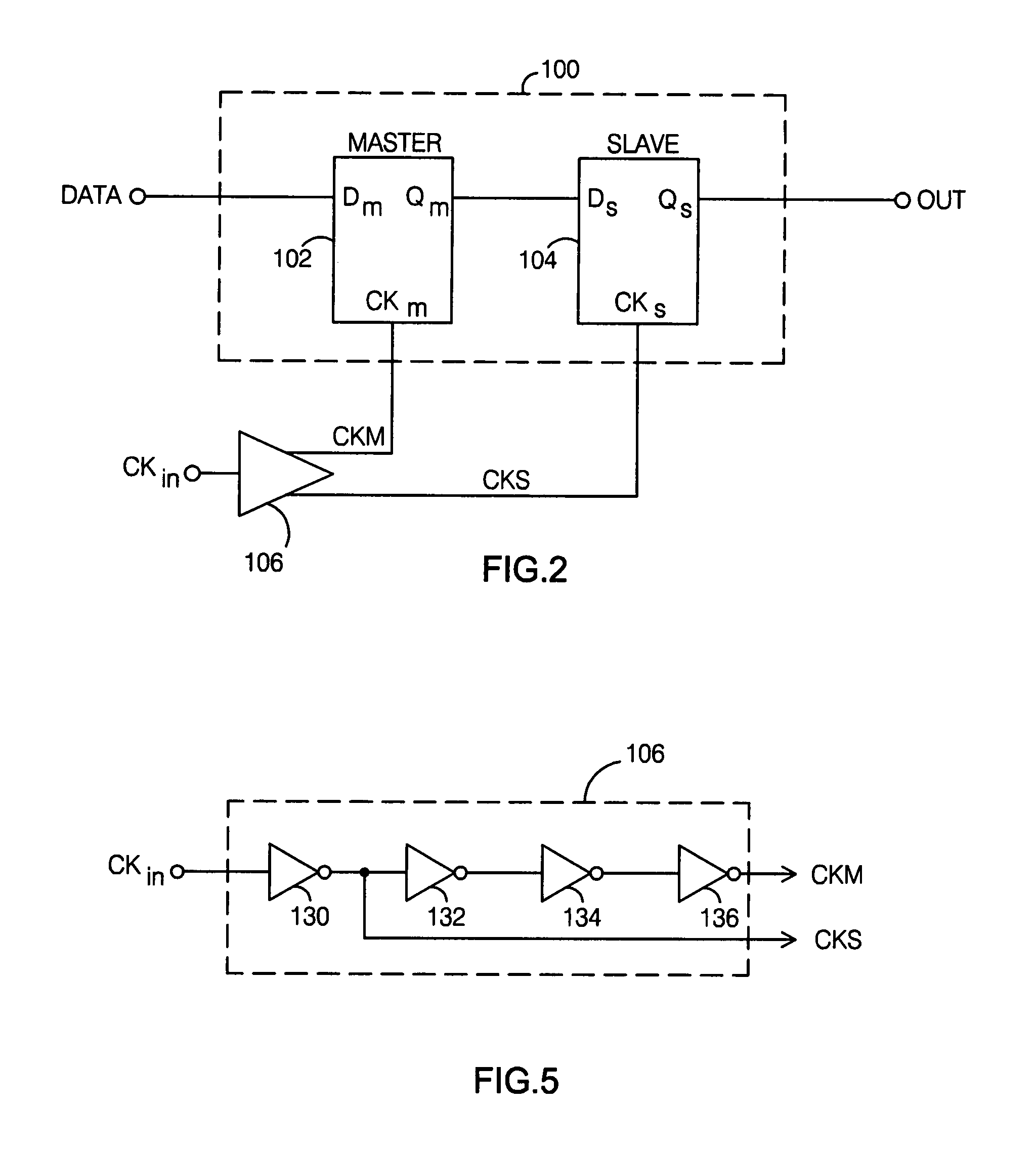
[0018]A block / schematic diagram of a master-slave flip-flop 100 per the present invention is shown in FIG. 2. The flip-flop includes a master latch 102 and a slave latch 104 having respective data inputs (Dm, Ds), data outputs (Qm, Qs), and clock inputs (CKm, CKs), with the data output of master latch 102 connected to the data input of slave latch 104. Master latch data input Dm serves as the flip-flop's data input, and data output Qs of slave latch 104 provides the flip-flop's data output.
[0019]The master and slave latches receive clock signals CKM and CKS, respectively, at their respective clock inputs. Each latch is arranged to be transparent when its clock signal is in a first state, and to latch a logic signal applied to its data input when its clock signal is in a second state.
[0020]The flip-flop also includes a clock buffer 106 which provides clock signals CKM and CKS. As discussed above, a master-slave flip-flop is typically driven with a pair of complementary clocks, such t...
PUM
 Abstract
Description
Claims
Application Information