Supercharge Your Innovation With Domain-Expert AI Agents!

Method of integrated circuit assembly

a technology of integrated circuits and components, applied in the direction of information storage, instruments, electrical devices, etc., can solve the problems of disconnection of two elements, small final thickness tb>2/b>, and paste being pushed towards the outside of the surface, and achieve strong solder bonding

Inactive Publication Date: 2008-08-12
STMICROELECTRONICS SRL
View PDF23 Cites 0 Cited by
  • Summary
  • Abstract
  • Description
  • Claims
  • Application Information

AI Technical Summary

Benefits of technology

[0016]Especially, the present invention aims at providing a novel method of soldering two integrated circuit elements which results in a strong solder bond, even under high operating temperatures and for large temperature variations.

Problems solved by technology

Another disadvantage of this pressure upon deposition is to expel the paste towards the outside of the surface to be soldered.
A disadvantage of this method is linked to the very small final thickness T2, especially as compared to the contact surfaces involved, which are relatively large.
Indeed, in the operation at high temperatures and during temperature variations, the heat coefficient difference between the two elements of different nature attached by soldering, combined with the small thickness of the soldering, can cause disconnection of the two elements.
Such disconnection results in malfunctions of the circuit in which it occurs.
But the high pressure during the deposition of the elements expels the paste outside the surface to be soldered, which results in new disadvantages, especially a problem of alignment of the elements, which tend to float.
It should be noted that these problems also arise when a soldering joint is created between a ceramic pad and a connection grid and between this pad and a sink.

Method used


Image

  • Method of integrated circuit assembly
  • Method of integrated circuit assembly
  • Method of integrated circuit assembly

Examples


Embodiment Construction

[0032]According to the present invention, the elements to be soldered are temporarily maintained at a predetermined distance from each other. This maintaining of a distance aims, in particular, at enabling the use of greater solder paste volumes without risking misalignment of the elements, even under a high mechanical pressure of deposition of the elements to be soldered.

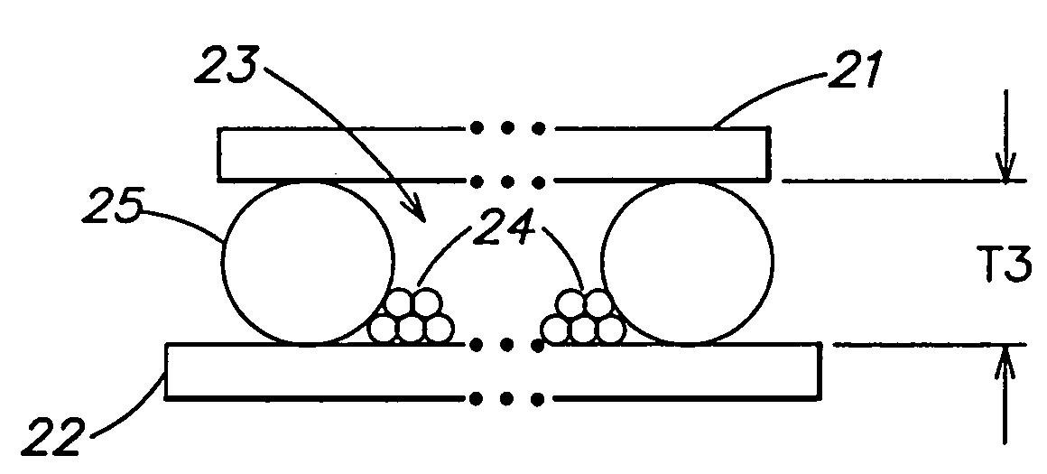
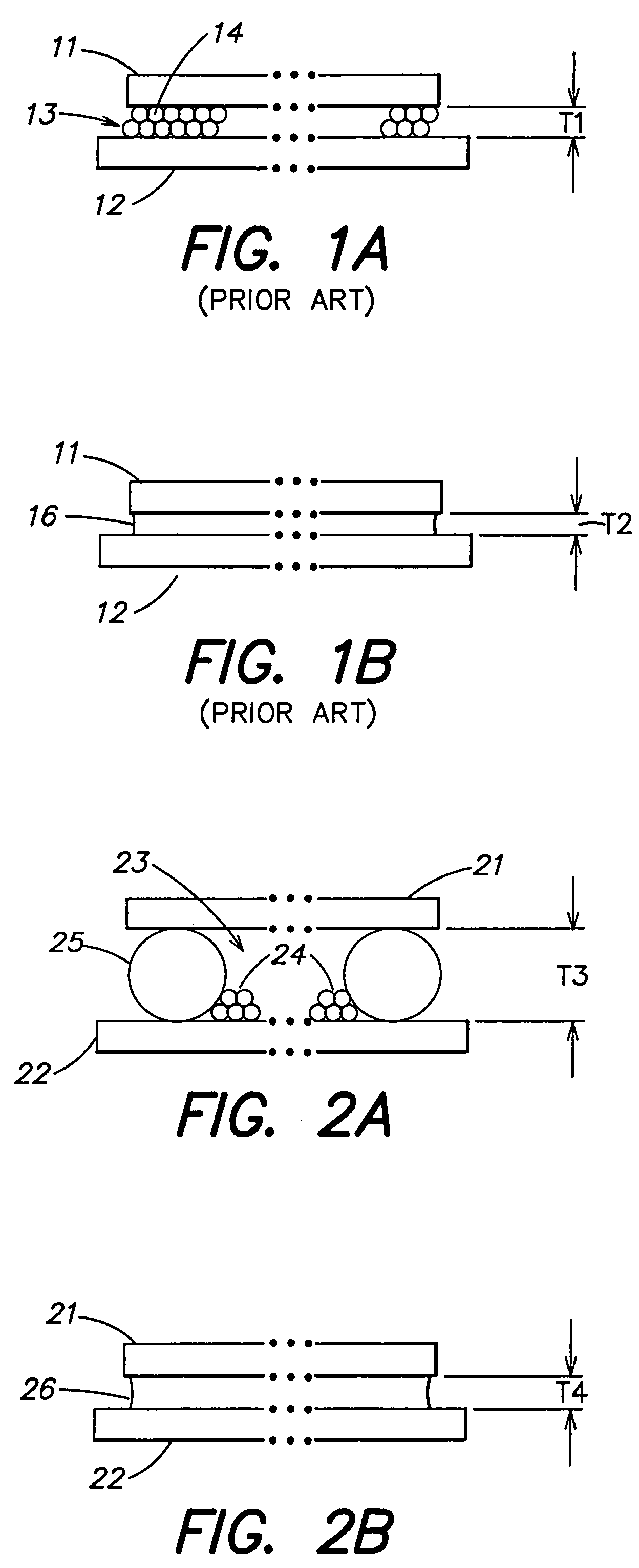
[0033]FIGS. 2A and 2B illustrate, in cross-section, respectively before and after the fusion, an embodiment of the present invention.

[0034]A soldering of a first element 21 on a second element 22 is desired to be performed by means of a solder paste 23.

[0035]According to this embodiment, paste 23 includes balls 25 of a much greater diameter than that of the other elements 24 of the paste, in particular, of other balls forming the bulk of the paste. These balls of greater diameter are formed of the same alloy as the other solder paste balls. They are spherical and calibrated in diameter. The proportion of such balls...


PUM

PropertyMeasurementUnit
diameteraaaaaaaaaa
diameteraaaaaaaaaa
diameteraaaaaaaaaa

Abstract

A method of integrated circuit assembly before encapsulation including at least one step of soldering, under mechanical pressure, a first element on a second element, including temporarily maintaining a predetermined spacing, at least partially without solder paste, between the surfaces to be assembled of the first and second elements.

Description

CROSS REFERENCE TO RELATED APPLICATIONS [0001]This application is a continuation of application Ser. No. 09 / 845,137, filed Apr. 30, 2001 now abandoned, which in turn is a continuation of application Ser. No. 09 / 364,529, filed Jul. 30, 1999, now U.S. Pat. No. 6,247,637 entitled METHOD OF INTEGRATED CIRCUIT ASSEMBLY, which prior applications are incorporated herein by reference.BACKGROUND OF THE INVENTION [0002]1. Field of the Invention[0003]The present invention relates to a method of integrated circuit assembly before encapsulation. More specifically, the present invention relates to soldering steps of such a method.[0004]2. Discussion of the Related Art[0005]In a conventional integrated circuit manufacturing method, each chip, resulting from the dicing of a semiconductive wafer on which are formed several chips, must be individually assembled on a heat sink. Each chip may be assembled on a connection grid, itself assembled on a heat sink, the sink and the connection grid being then...

Claims


Application Information

Patent Timeline
Patent Type & Authority Patents(United States)
IPC IPC(8): B23K31/02G11C15/04H01L21/48H01L21/60H01L21/98
CPCG11C15/04H01L21/4882H01L24/31H01L24/83H01L25/50H01L2924/00013H01L2224/8319H01L2224/83801H01L2924/01047H01L2924/0105H01L2924/01057H01L2924/01058H01L2924/01061H01L2924/01079H01L2924/01082H01L2924/14H01L2924/014H01L2224/29099
Inventor FARRONI, JEAN-PAUL
Owner STMICROELECTRONICS SRL
Features
  • R&D
  • Intellectual Property
  • Life Sciences
  • Materials
  • Tech Scout
  • Unparalleled Data Quality
  • Higher Quality Content
  • 60% Fewer Hallucinations
Learn More