Carrier for LTCC components

a carrier and cofired ceramic technology, applied in the direction of printed circuit aspects, printed circuit stress/warp reduction, semiconductor/solid-state device details, etc., can solve the problems of difficult inability to use gold over nickel as a finish for most ltcc designs, and difficulty in visual inspection of solder joints, so as to reduce the amount of pcb real estate, reduce the amount of metal leaching, and increase the resistance to thermal stress and mechanical shock

Active Publication Date: 2015-10-20
SCI COMPONENTS
View PDF2 Cites 1 Cited by
  • Summary
  • Abstract
  • Description
  • Claims
  • Application Information

AI Technical Summary

Benefits of technology

[0020]The improved carrier for an LTCC component described herein provides attachment of an LTCC component to a PCB with increased resistance to thermal stress and mechanical shock, reduced leaching of metal from contact pads, and a visible solder joint to aid in quality inspection after reflow soldering. The carrier provides these benefits cost-effectively and with minimal increase in required PCB real estate.
[0021]The carrier has a flat body composed of a mixture of thermosetting polymer, woven glass fiber and ceramic, or pure ceramic. The top and bottom surfaces of the carrier have metal contact pads aligned over each other, spaced to correspond to the interconnect pads of the LTCC component which will be bonded to the carrier. Each pair of top and bottom contact pads is electrically connected by at least one conductive via passing through the body of the carrier, except in the ceramic carriers. The material of the contact pads is gold over nickel rather than the standard PdAg alloy metal, thus preventing metal leaching during reflow soldering and providing a stronger solder bond. Solder is deposited on the top pads to prepare them for attachment to the LTCC component, which is further secured to the carrier by a layer of adhesive on the carrier top surface. This adhesive is preferably an epoxy and serves to further improve bonding between the LTCC component and the carrier, making the assembly more resistant to thermal stress and mechanical shock. Since the material of the LTCC component and the material of the non-ceramic carriers have very different CTE, a slot is made through the non-ceramic carrier between the top and bottom surfaces to allow better accommodation of differences in thermal expansion. Castellations are present on at least some pairs of opposite sides of the carrier, with metallization in the castellations providing additional surface area for the reflow solder joint with the PCB, and a means for visually inspecting the quality of the solder joint. To prevent solder spreading from the metallization, a gap is present in the metallization preferably near the top contact pads thus preventing poor solder joint quality between the carrier and the LTCC component.OBJECTS AND FEATURES OF THE INVENTION
[0023]It is another object of the invention to provide a carrier for an electronic component where the carrier doesn't impair high frequency performance.
[0024]It is yet another object of the invention to provide a carrier for an electronic component having improved resistance to failure from thermal stress and mechanical shock.
[0025]It is a feature of the invention to provide a carrier for an electronic component that permits easier visual inspection of solder joints after soldering to a PCB.

Problems solved by technology

Historically, gold over nickel has not been available as a finish for most LTCC designs.
One quality problem in reflow soldering of LTCC components to PCBs is the inspection of solder joints.
The typical interconnect termination for an LTCC component is located on the bottom of the component and thus visual inspection of the solder joints is difficult when the component has been soldered in place on a PCB.
One technique to allow easier visual inspection of the solder joints involves welding or brazing metal leads to the terminations, though this adds expense and the risk of damage to the terminations.
Another technique is to add solderable wraparound metal leads to the LTCC package, which results in reduced real estate for circuitry on the top layer and adds lead inductance, thus reducing high frequency performance.
Another quality problem for LTCC components is in mitigating thermal stress and mechanical shock, which can cause interconnect termination joint failure or even cracking of the component.
The coefficient of thermal expansion (CTE) of ceramic and silicon components is sufficiently different from the CTE of typical epoxy fiberglass PCBs that this mismatch can cause solder joint failure with changes in temperature.
The CTE mismatch problem is worse for larger components where the amount of thermally induced mechanical stress is greater.
This substrate requires numerous manufacturing steps and is a mechanically complex solution to the problem, and since the conductive posts are under the component, provides no improvement to inspection of the resulting solder joints.
Since the solderable contacts are under the component it provides no improvement to inspection of the resulting solder joints.
However, in either version the solder joints are under the substrate and thus difficult to inspect.
This approach causes the footprint of the PCB to be different than that of the component, which is a major drawback.
This approach causes the footprint of the PCB to be different than that of the component, which is not acceptable in existing PCB designs and in addition, the brazing operation could result in cracking of the LTCC material.
The disadvantage of this approach is that the metal clips will increase circuit inductance and thus limit high frequency operation, and also have to be manufactured as separate parts and then assembled onto the dielectric frame.
This approach has the disadvantage of requiring specialized manufacturing for the PCB, requires additional real estate, and also does not address the problem of solder joint inspection since the solder joints are either under the component or are situated at leads extending outwards which lower the usable frequency range of the circuit.
All three of these inventions provide solder connections under the interposers or substrates and thus provide no improvement in ability to inspect the solder joints.
This carrier has a generally simple and useful form but has leads long enough to impose limits on high frequency operation and by being substantially larger than the surface mount component is inefficient for mounting the component with a minimal increase in PCB real estate.

Method used


Image

  • Carrier for LTCC components
  • Carrier for LTCC components
  • Carrier for LTCC components

Examples


Embodiment Construction

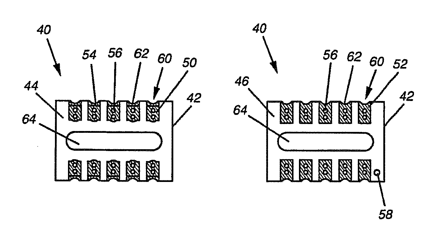
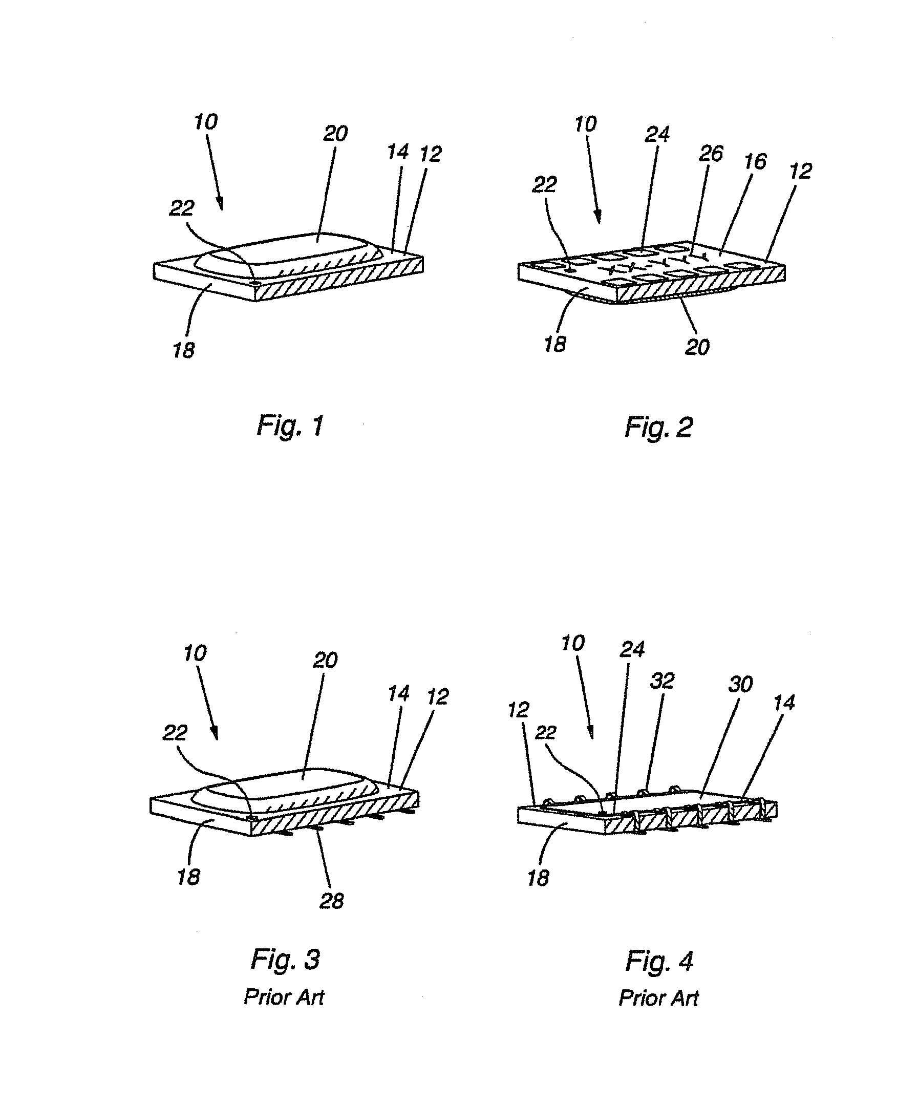
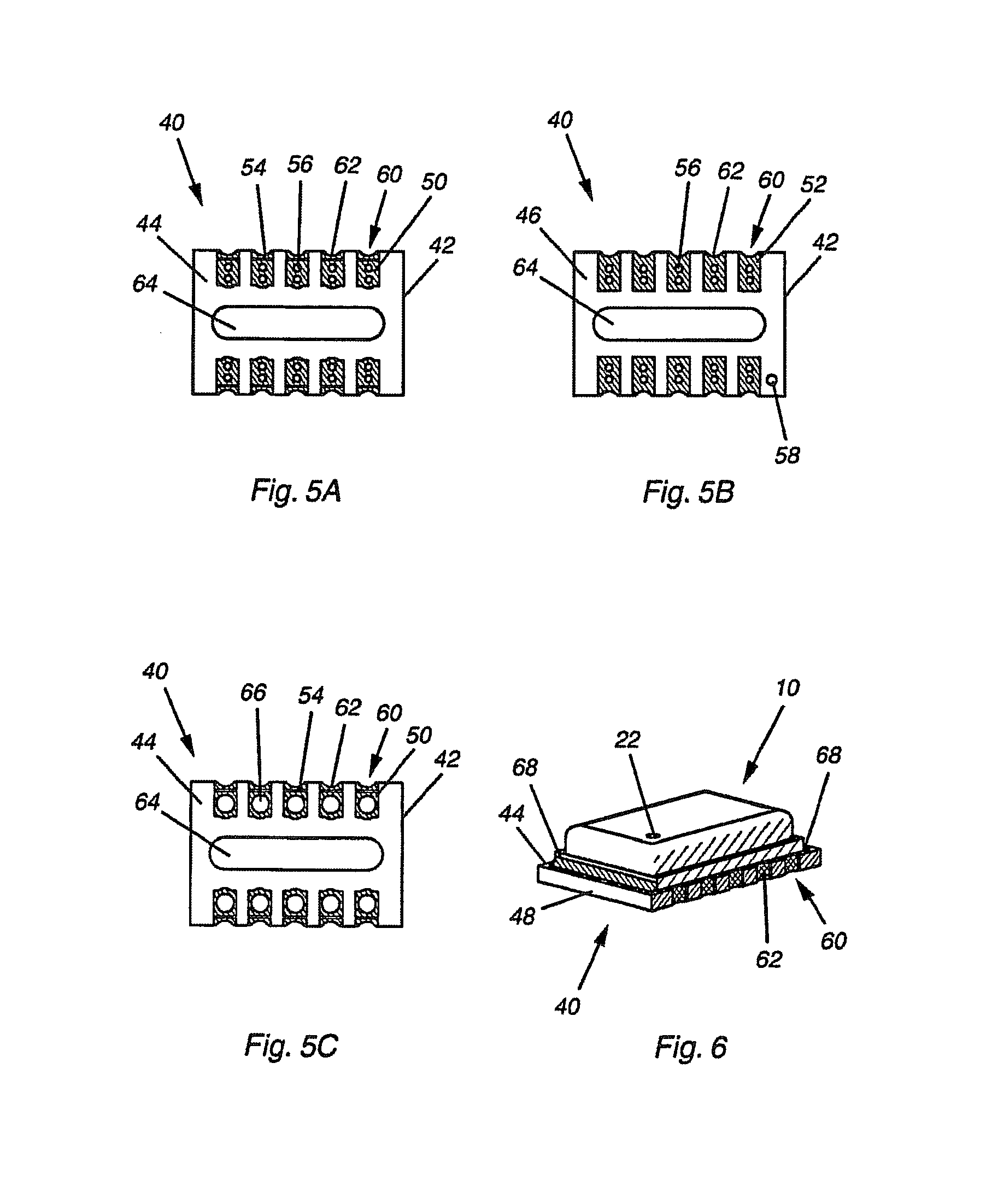
[0047]Referring to FIGS. 1 and 2, an LTCC component 10 is shown with a plastic-encapsulated semiconductor die 20 mounted on the LTCC top surface 14. Mounting orientation of the component 10 is shown by the orientation mark 22 placed on both the LTCC top surface 14 and the LTCC bottom surface 16. The LTCC bottom surface 16 also features an identification mark 26, and conductive termination pads 24 with which the component 10 is soldered to a substrate, typically a PCB. The component body 12 is composed of low temperature co-fired ceramic (LTCC) and has a different coefficient of thermal expansion (CTE) than the fiberglass and epoxy PCB that it is soldered to. Additionally, the standard material that the conductive termination pads 24 are made of is a palladium silver alloy (PdAg) which has been found to leach out during successive heating cycles such as those experienced during reflow soldering. Both the CTE mismatch and the leaching of metal from the conductive termination pads 24 c...


PUM


Abstract

An LTCC carrier composed of thermosetting polymer, woven glass fiber and ceramic has gold over nickel contact pads on top and bottom surfaces and conductive vias therethrough between aligned pairs of top and bottom pads. The vias prevent undesirable inductive paths from limiting high frequency operation of the circuitry. Solder deposits on the top pads attach the LTCC component, which is further secured to the carrier by epoxy, thus improving resistance to thermal stress and mechanical shock. A slot through the carrier body between top and bottom surfaces further reduces thermal stress and mechanical shock. Metallized castellations on opposite carrier sides provide additional surface area for reflow solder joints with the PCB, and a means for visually inspecting the solder joint quality. A gap in the metallization on the top layer of the carrier prevents solder spreading during multiple soldering cycles, which may result in poor solder joints.

Description

[0001]This is a divisional application of currently pending U.S. patent application Ser. No. 12 / 655,318 filed Dec. 28, 2009.BACKGROUND OF THE INVENTION[0002]1. Field of the Invention[0003]This invention relates to carriers for electronic components and in particular to carriers for low temperature co-fired ceramic (LTCC) components.[0004]2. Description of the Prior Art[0005]Surface Mount Technology (SMT) is used by the electronics industry as a mass production technique for attaching electronic components to printed circuit boards (PCBs) by reflow soldering. The electronics industry has a continuing need to shrink components in order to decrease the PCB area needed for circuitry, and to fit more circuitry into a given area. One method of shrinking components is to use Low Temperature Co-fired Ceramic, (LTCC) which allows circuitry to be distributed in multiple stacked layers rather than being spread out in a single layer. Examples of LTCC circuitry, are disclosed in U.S. Pat. Nos. 7...

Claims


Application Information

Patent Timeline
Patent Type & Authority Patents(United States)
IPC IPC(8): H05K7/10H05K7/12H05K1/11H05K1/09
CPCH05K1/111H05K1/09H05K1/113H05K2201/0753H05K2201/032H01L23/15H01L23/13H01L23/49805H01L2924/0002H05K1/0271H05K1/0306H05K2201/10378H01L2924/00
Inventor KAYLIE, HARVEY L.RAKLYAR, ARON
Owner SCI COMPONENTS
Why Eureka
Try Eureka