Supercharge Your Innovation With Domain-Expert AI Agents!

Programmable random logic arrays using PN isolation

a random logic and pn isolation technology, applied in the field of integrated circuit devices of random logic, can solve the problems of relatively complex design and manufacturing processes, and achieve the effect of reducing fabrication costs and simplifying fabrication

Active Publication Date: 2008-09-02
TAIWAN SEMICON MFG CO LTD
View PDF9 Cites 0 Cited by
  • Summary
  • Abstract
  • Description
  • Claims
  • Application Information

AI Technical Summary

Benefits of technology

This approach simplifies the fabrication process, reduces parasitic transistor formation, and lowers costs by enabling generic front-end precursors and flexible device definition, while maintaining performance as voltage thresholds and geometries shrink.

Problems solved by technology

One challenge to the manufacturers of such circuits is to provide each customer with a circuit that is or can be tailored to the specific needs of that customer.
While various ways are known to provide random logic, they tend to require relatively complex designs and manufacturing processes.

Method used


Image

  • Programmable random logic arrays using PN isolation
  • Programmable random logic arrays using PN isolation
  • Programmable random logic arrays using PN isolation

Examples


Embodiment Construction

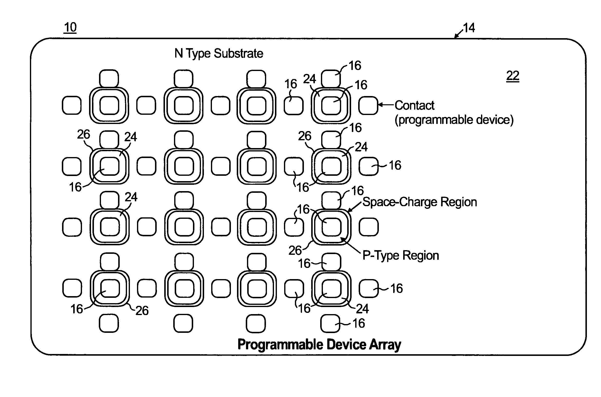
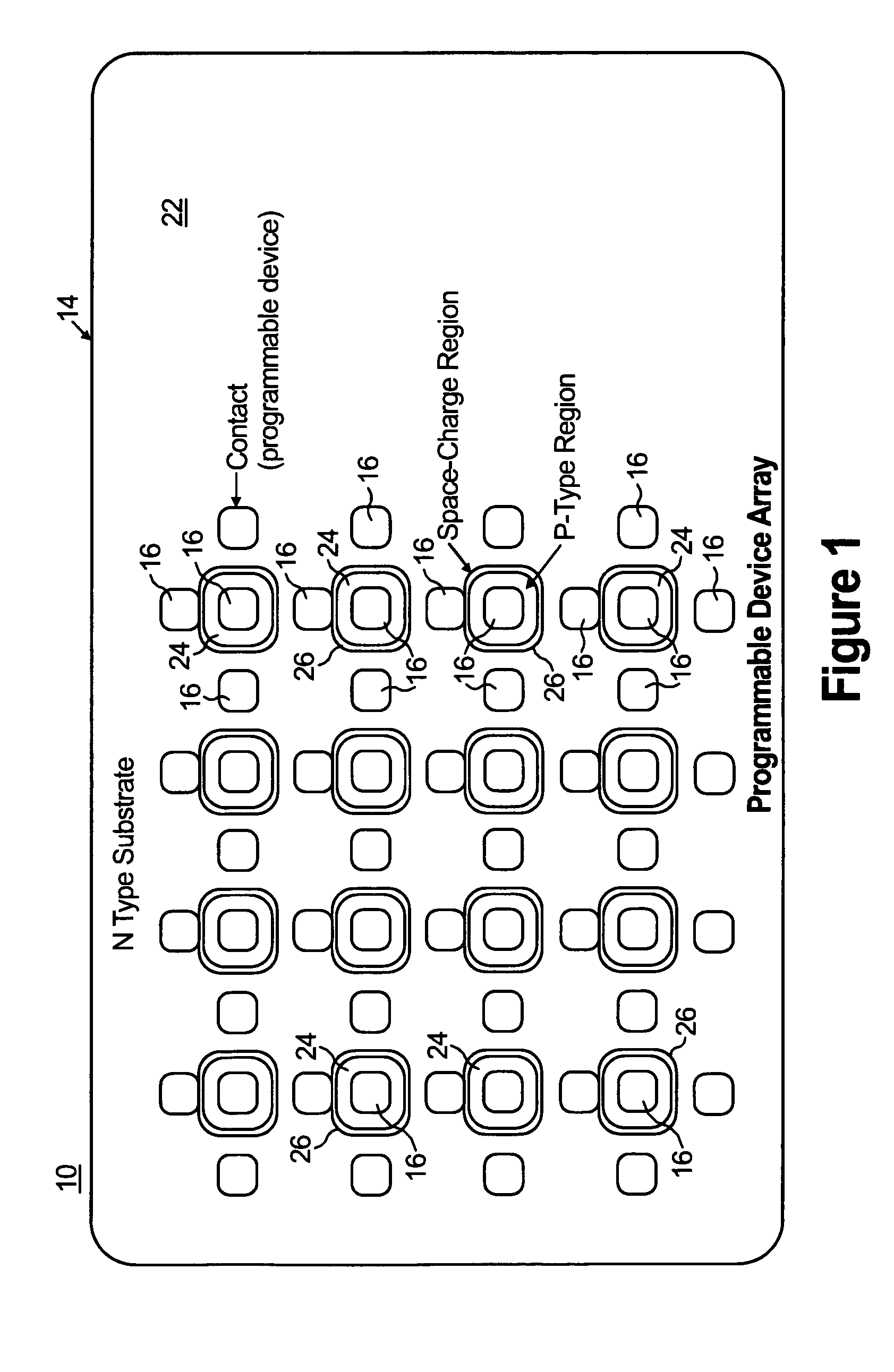
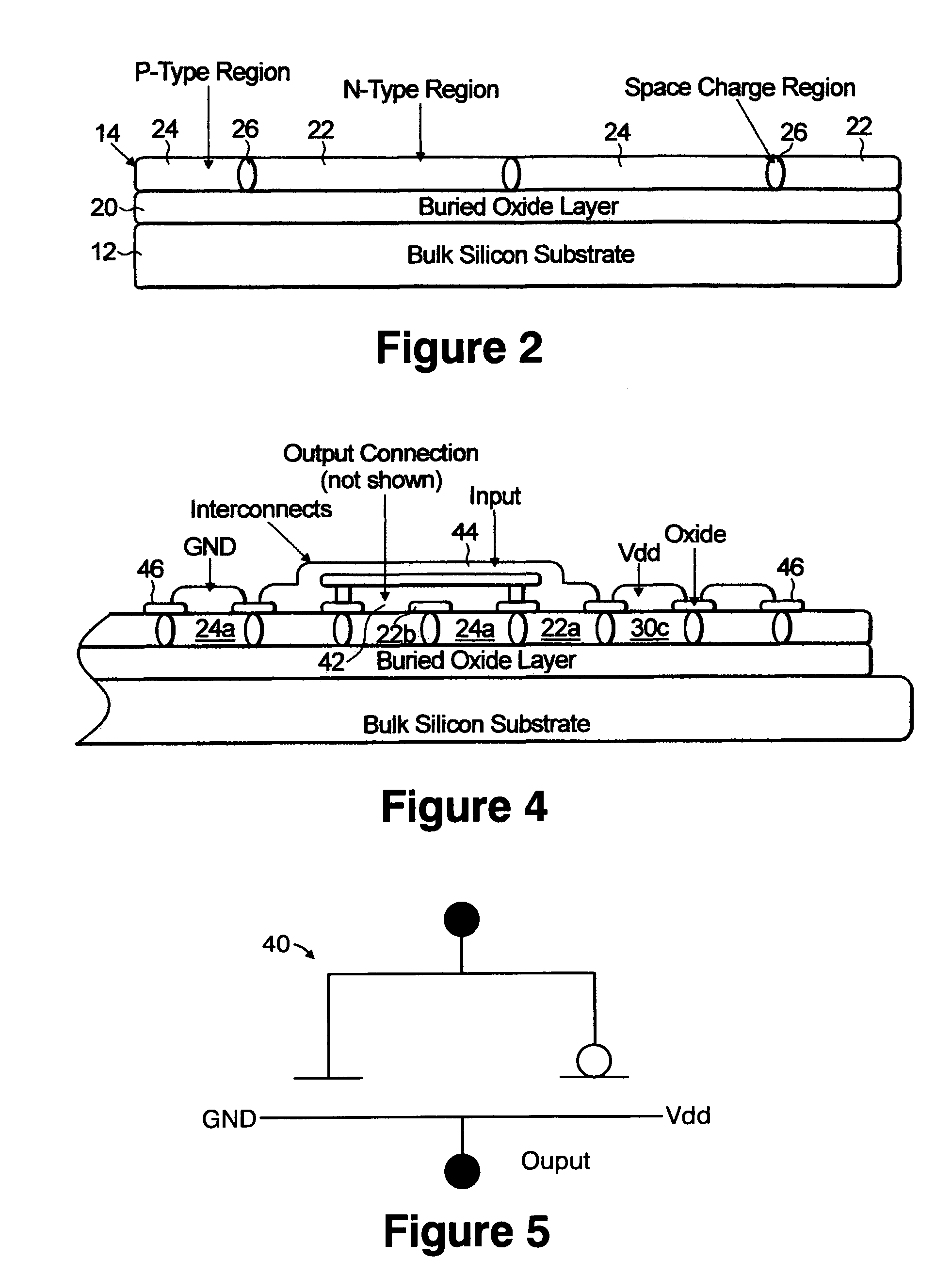
[0023]The invention will now be described by reference to the accompanying figures. In these figures, various aspects of the structures have been shown and schematically represented in a simplified manner to more clearly describe and illustrate the invention. For example, the figures are not intended to be to scale. In addition, various aspects of the structures are illustrated as having particular shapes; however, as those skilled in the art will appreciate, the invention is not limited to constructions of any particular shape.

[0024]As mentioned above, this invention generally relates to integrated circuits or semiconductor structures or wafers. FIGS. 1 and 2 show a semiconductor structure or wafer 10 comprising lower substrate 12, upper semiconductor layer 14, and a series of contacts, generally referenced at 16; and preferably, structure 10 further comprises oxide layer 20 between substrate 12 and layer 14.

[0025]Upper layer 14, in turn, includes N-type region 22, an array of P-ty...


PUM


Abstract

Disclosed are a programmable, random logic device array, and a method of forming such a device. The device comprises a substrate, and a semiconductor layer above the substrate. That semiconductor layer, in turn, includes a first region of a first semiconductor type, an array of spaced apart second regions of a second semiconductor type, and a plurality of space-charge regions. Each of the space charge regions extends around a respective one of the second regions and separates that one of the second regions from the first region of the semiconductor layer. The programmable, random, logic device array further comprises first and second sets of contacts. The first set of contacts are in electrical contact with areas of said first region of the semiconductor layer, and the second set of contacts are in electrical contact with the second regions.

Description

BACKGROUND OF THE INVENTION[0001]1. Field of the Invention[0002]This invention generally relates to integrated circuits. More specifically, the invention relates to random logic integrated circuit devices, and to methods for making such circuits.[0003]2. Background Art[0004]Integrated circuits are an essential part of digital systems, such as computers. One challenge to the manufacturers of such circuits is to provide each customer with a circuit that is or can be tailored to the specific needs of that customer.[0005]There are several ways to address this challenge. One way is to provide circuits that are programmable or have random logic. Logic can be designed and fixed, as in a gate array (GA) device, so that earlier, or “front end” (FE), process steps used in the manufacture of the circuits are quite generic, in particular, with respect to implantation and contact. Personalization of the devices can be entirely or substantially accomplished in the later, or “back end” (BE), metal...

Claims


Application Information

Patent Timeline
Patent Type & Authority Patents(United States)
IPC IPC(8): H01L27/12
CPCH01L21/84H01L27/0207H01L27/1203H01L27/118H01L27/10
Inventor BHATIA, HARSARAN S.KLINE, ERIC
Owner TAIWAN SEMICON MFG CO LTD
Features
  • R&D
  • Intellectual Property
  • Life Sciences
  • Materials
  • Tech Scout
  • Unparalleled Data Quality
  • Higher Quality Content
  • 60% Fewer Hallucinations
Learn More