Electromagnetic radiation absorber
- Summary
- Abstract
- Description
- Claims
- Application Information
AI Technical Summary
Benefits of technology
Problems solved by technology
Method used
Image
Examples
Embodiment Construction
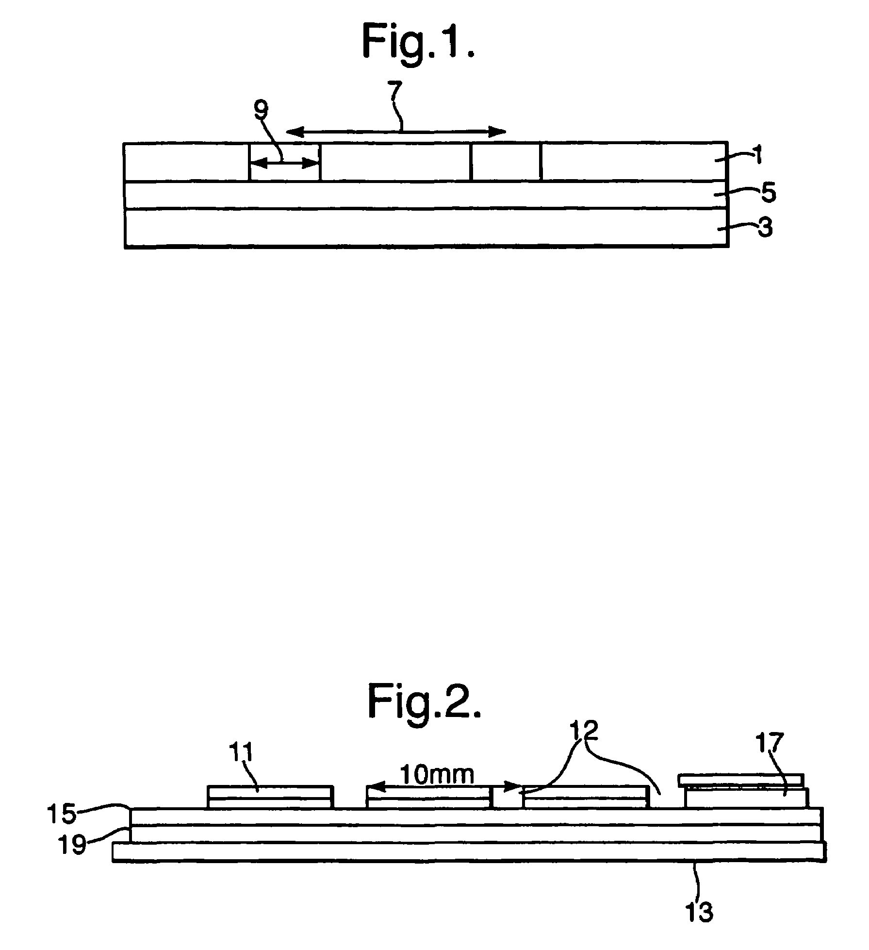
[0049]Turning to FIG. 1, a multi-layer electromagnetic radiation absorbing material comprises a first conductor layer 1 and a second conductor layer 3. Conductors 1,3 sandwich a dielectric core 5.
[0050]The first conductor layer 1 has a number of slits of separation 7 and width 9.
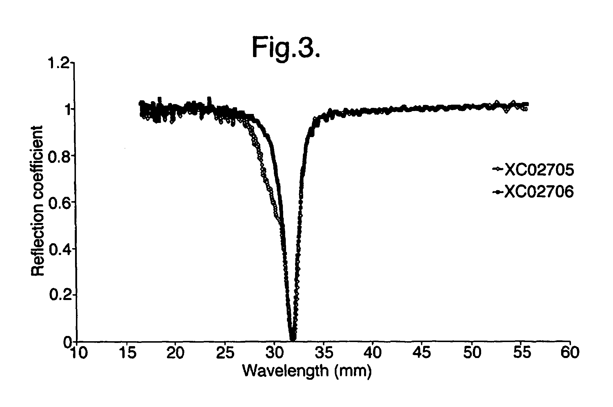
[0051]In an example of an absorber constructed for use as a microwave absorber the thickness of each of the copper conductor layers 1 and 3 was 18 microns and the thickness of the dielectric was approximately 360 microns. Slit separation was 10 mm and slit width 50-400 microns. Such a construction lead to absorption at around a wavelength of 40 mm. It should be noted that the total thickness of the material (approx. 400 microns) is around 1 / 100th the wavelength of the incident radiation.
[0052]FIG. 2 shows a further example of a radiation absorber according to the present invention. In this case copper layers 11 and 13 sandwich a polyester layer 15. The upper copper layer 11 contains a slit arrangement 12.
[00...
PUM
 Abstract
Description
Claims
Application Information


