Nitride semiconductor laser element and method for manufacturing same
a laser element and semiconductor technology, applied in the field of nitride semiconductor laser elements, can solve the problems of cracks, current leakage, and difficulty in controlling optical confinement in horizontal-lateral mode, and achieve the effects of reducing stress, prolonging service life characteristics, and stabilizing optical confinemen
- Summary
- Abstract
- Description
- Claims
- Application Information
AI Technical Summary
Benefits of technology
Problems solved by technology
Method used
Image

Examples
example 1
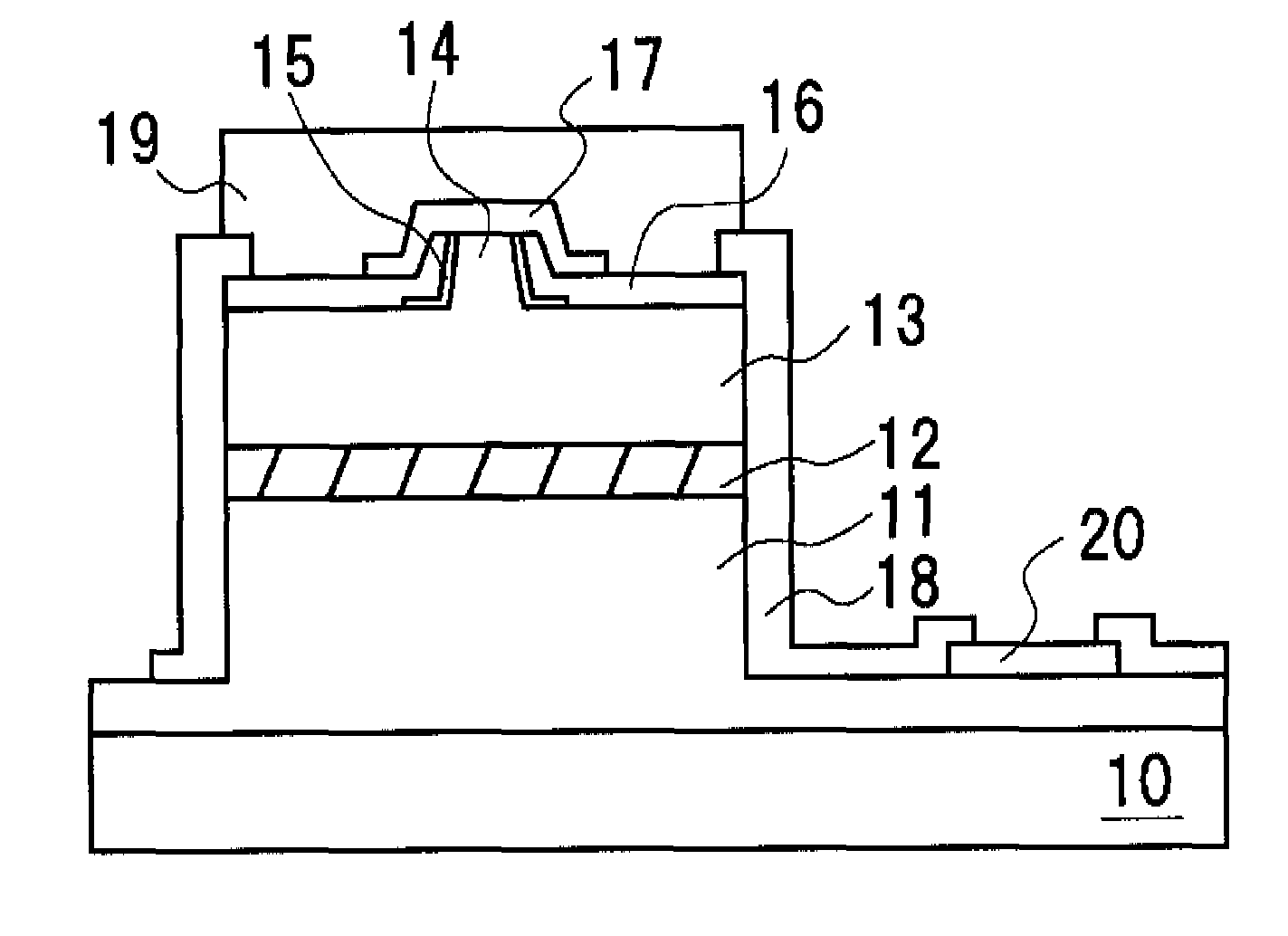
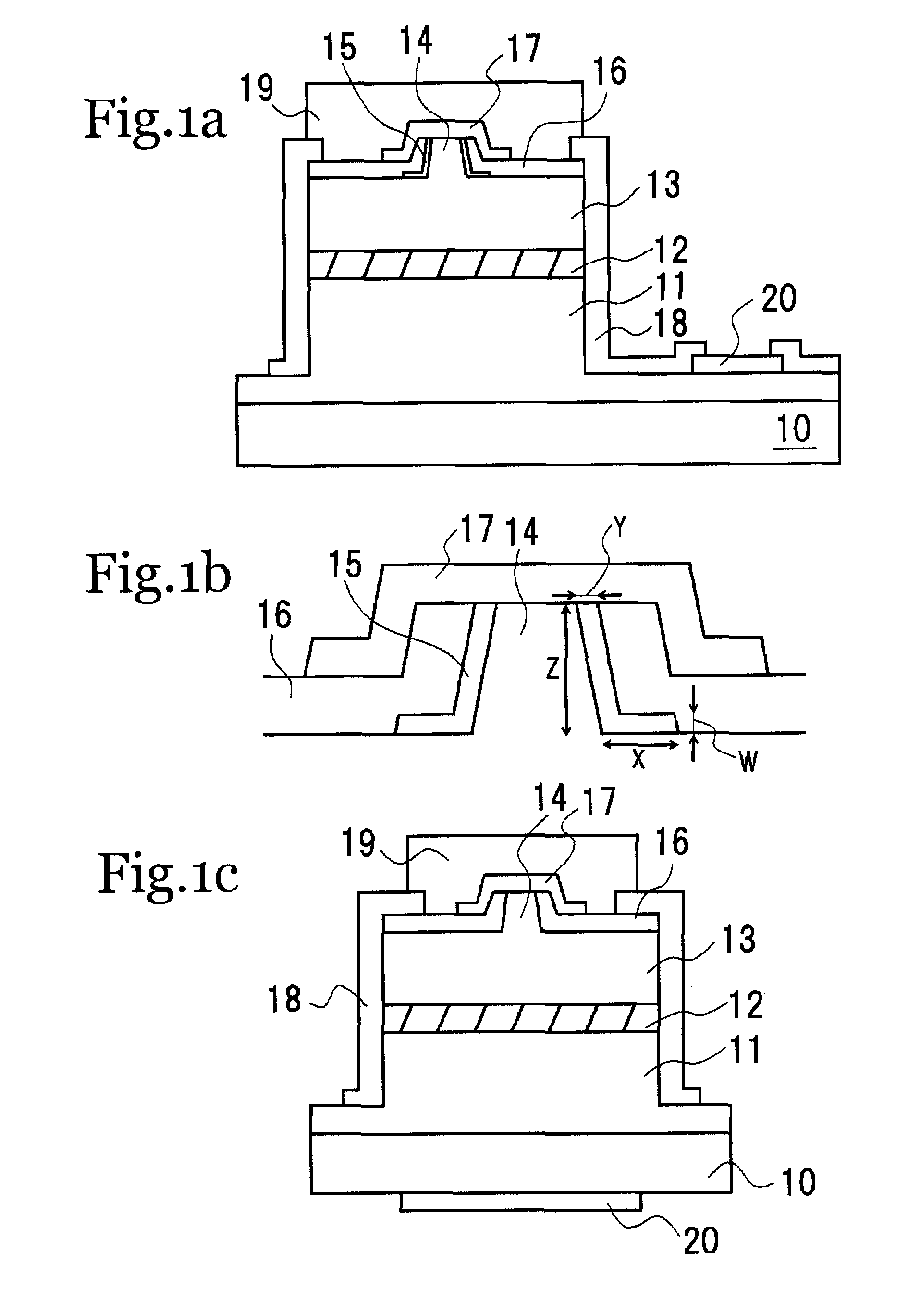
[0084]The laser element in this example oscillates in a band of 390 nm and under, and as shown in FIGS. 1a and 1b, a first buffer layer (100 nm) composed of silicon-doped Al0.02Ga0.98N and a second buffer layer (150 nm) composed of silicon-doped In0.1Ga0.9N are formed on a substrate 10 composed of n-type GaN. Over this, an n-side cladding layer (0.7 μm) composed of silicon-doped Al0.11Ga0.89N and an n-side light guide layer (0.15 μm) composed of undoped Al0.06Ga0.94N are formed as an n-side semiconductor layer 11, and a barrier layer (7 nm) composed of silicon-doped Al0.15Ga0.85N, a well layer (10 nm) composed of undoped In0.01Ga0.09N, and a barrier layer (5 mm) composed of Al0.15Ga0.85N are formed as an active layer 12 composed of a single quantum well. Over this are formed a p-side cap layer (10 nm) composed of magnesium-doped p-side Al0.30Ga0.70N, a p-side light guide layer (0.15 μm) composed of undoped Al0.06Ga0.94N, a p-side cladding layer composed of a superlattice layer with ...
example 2
[0106]Substantially the same element as in Example 1 is formed in the same way, except that in this example the first protective film has a two-layer structure with ZrO2 of different film quality.
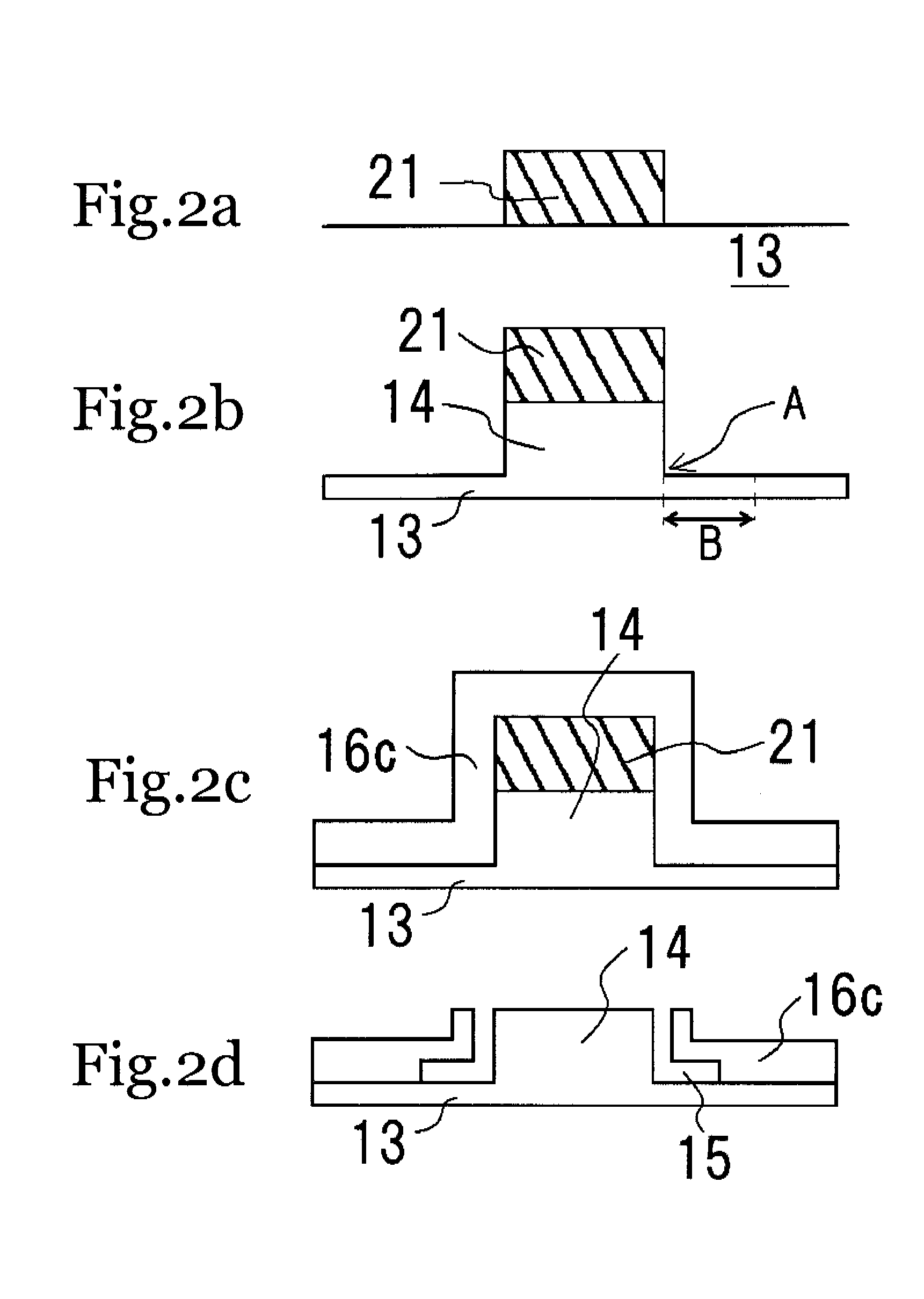
[0107]First, just as in Example 1, a ridge is formed on the nitride semiconductor layer surface using a mask pattern, and as shown in FIG. 3a, a ZrO2 film with a thickness of 10 nm is formed as a lower layer 16a of the first protective film using a magnetron sputtering device. Next, a ZrO2 film with a thickness of 90 nm is formed as an upper layer 16b using an ECR sputtering device.
[0108]The first protective films 16a and 16b thus obtained are annealed at 300° C. and immersed in BHF for 15 minutes, which, as shown in FIG. 3b, dissolved away the mask pattern formed on the p-side contact layer, and the first protective film on the p-side contact layer is removed along with the mask pattern by lift-off method. Further, a cavity is formed in this step by etching the lower layer 16a and upper la...
example 3
[0110]Substantially the same element as in Example 1 is formed in the same way, except that in this example the first protective film has a two-layer structure composed of different materials.
[0111]First, just as in Example 1, a ridge is formed on the nitride semiconductor layer surface using a mask pattern, and an SiO2 film with a thickness of 10 nm is formed as the lower layer of the first protective film using an ECR sputtering device. Next, a ZrO2 film with a thickness of 40 nm is formed as the upper layer using an ECR sputtering device.
[0112]The first protective film thus obtained is annealed at 400° C. and immersed in BHF for 15 minutes, which dissolved away the mask pattern formed on the p-side contact layer, and the first protective film on the p-side contact layer is removed along with the mask pattern by lift-off method. Further, a cavity is formed in this step at the ridge side faces and the ridge bottom face by etching the SiO2 film serving as the lower layer and the ZrO...
PUM
| Property | Measurement | Unit |
|---|---|---|
| cavity height | aaaaa | aaaaa |
| cavity height | aaaaa | aaaaa |
| height | aaaaa | aaaaa |
Abstract
Description
Claims
Application Information