Film bulk acoustic wave resonator and manufacturing method thererof

a film and acoustic wave technology, applied in the direction of impedence networks, generators/motors, device material selection, etc., can solve the problems of too large to be implemented as a compact and light integrated circuit on a semiconductor substrate, difficult to manufacture the saw filter operation, and difficult to implement a compact dielectric filter into a monolithic microwave integrated circuit (mmic). , to achieve the effect of improving the degree of integration, reducing manufacturing processes, and simple structur

Active Publication Date: 2008-09-09
SAMSUNG ELECTRONICS CO LTD
View PDF10 Cites 13 Cited by
  • Summary
  • Abstract
  • Description
  • Claims
  • Application Information

AI Technical Summary

Benefits of technology

[0033]The present invention has been made to overcome the above-mentioned problems in the related art. Accordingly, it is a first aspect of the present invention to provide a film bulk acoustic resonator of a simple structure, reduced manufacturing processes and an improved degree of integration.

Problems solved by technology

However, they are too big to be implemented as a compact and light integrated circuit on a semiconductor substrate.
However, it is difficult to implement a compact dielectric filter into a Monolithic Microwave Integrated Circuit (MMIC).
However, it is not easy to manufacture the SAW filter operating at more than a super high frequency (5 GHz or higher) band due to manufacturing process restrictions.
The Bragg reflector type FBAR fabrication method is disadvantageous in that it is difficult to form a reflection layer structure having an accurate thickness of four or more reflection layers for total reflection and it takes long time and cost to manufacture, although there are advantages in that it is structurally rigid and no stress due to bending is generated.
An FBAR element thus structured is not practical due to its very weak structure and a low recovery rate.
Furthermore, in manufacturing the membrane, the sacrificial layer needs to be slanted, which causes a weak structure due to a high remaining stress of the membrane.
In case of wet etching, it is hard to remove the etchant.

Method used


Image

  • Film bulk acoustic wave resonator and manufacturing method thererof
  • Film bulk acoustic wave resonator and manufacturing method thererof
  • Film bulk acoustic wave resonator and manufacturing method thererof

Examples


Embodiment Construction

[0048]Hereinafter, exemplary embodiments of the present invention will be described in detail with reference to the accompanying drawings.

[0049]In the following description, same drawing reference numerals are used for the same elements even in different drawings. The matters defined in the description, such as a detailed construction and elements, are only provided to assist in a comprehensive understanding of the invention. Thus, it is apparent that the present invention can be carried out without those defined matters. Also, well-known functions or constructions are not described in detail since they would obscure the invention in unnecessary detail.

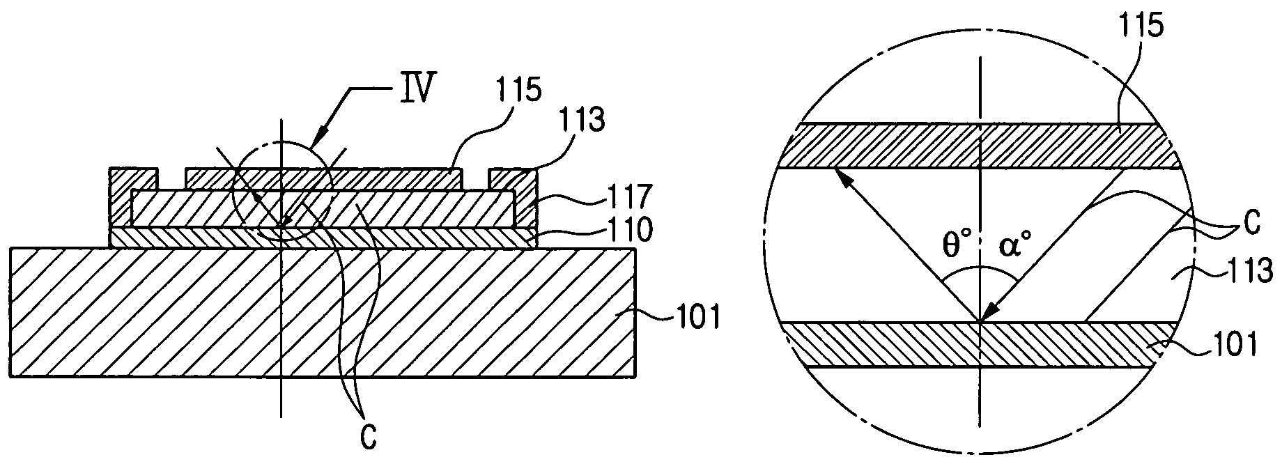
[0050]FIG. 3 is a cross-sectional view illustrating a structure of FBAR according to an embodiment of the present invention, and FIG. 4 is an enlarged view of display part IV of FIG. 3;

[0051]Referring to FIG. 3, a FBAR comprises a substrate 101, a lower electrode 110, a piezoelectric membrane 113 and an upper electrode 115.

[0052]The s...


PUM


Abstract

A film bulk acoustic resonator includes a substrate; a lower electrode formed on top of the substrate; a piezoelectric membrane formed on top of the lower electrode and having a crystallographic axis so inclined as to generate a total reflection when an acoustic wave advances toward the lower electrode; and an upper electrode formed on top of the piezoelectric membrane.

Description

CROSS-REFERENCE TO RELATED APPLICATIONS[0001]This application claims priority under 35 U.S.C. § 119(a) from Korean Patent Application No. 2005-64803, filed on Jul. 18, 2005, the entire contents of which are incorporated herein by reference.BACKGROUND OF THE INVENTION[0002]1. Field of the Invention[0003]The present invention relates in general to a film bulk acoustic wave resonator and manufacturing method thereof.[0004]2. Description of the Related Art[0005]For radio frequency (RF) band, a dielectric resonator, a metal cavity resonator and a piezoelectric thin film resonator (FBAR) are used.[0006]These resonators are superior in terms of a small insertion loss, a frequency characteristic or temperature stability.[0007]However, they are too big to be implemented as a compact and light integrated circuit on a semiconductor substrate.[0008]When compared with the dielectric resonator or the metal cavity resonator, the FBAR can be manufactured to be compact and can be implemented on a si...

Claims


Application Information

Patent Timeline
Patent Type & Authority Patents(United States)
IPC IPC(8): H03H9/15H03H9/17H03H9/54H01L41/09H01L41/18H01L41/187H01L41/22H01L41/23H01L41/316H03H3/02
CPCH03H3/02H03H9/172H03H9/02118H03H9/02015H03H9/24
Inventor KIM, DUCK-HWANKIM, CHUL-SOOPARK, YUN-KWONSUL, SANG-CHULHA, BYEOUNG-JUSONG, IN-SANG
Owner SAMSUNG ELECTRONICS CO LTD
Why Eureka
Try Eureka