
Lithographic apparatus

a technology of lithographic projection and lithographic device, which is applied in the direction of electrical apparatus, printing, instruments, etc., can solve the problems of inability to accurately obscure the patterning device inability to use conventional masking device to accurately obscure the patterning device, and failure of conventional masking device further. achieve the effect of improving the selectivity of parts, cost-effectiveness, and optimizing space utilization

Active Publication Date: 2008-09-09
ASML NETHERLANDS BV
View PDF38 Cites 4 Cited by
  • Summary
  • Abstract
  • Description
  • Claims
  • Application Information

AI Technical Summary

Benefits of technology

The present invention provides an improved apparatus and method for selectively imaging a patterning device onto a substrate in a lithographic process. The apparatus includes an illumination system, a support structure for the patterning device, a projection system, and a spatial filter. The spatial filter selectively obstructs a portion of the patterning device's beam of radiation, increasing the accuracy of the patterning process. The apparatus can be used in various manufacturing processes, such as the manufacture of ICs, and can be cost-effective and space-efficient. The technical effects of the invention include improved accuracy and efficiency of patterning, reduced dynamic disturbances, and increased flexibility in applications.

Problems solved by technology

Conventional masking devices may have drawbacks.
Further, conventional masking devices cannot be relied upon to accurately obscure the patterning device.
As higher scanning speeds are demanded, conventional masking devices fail further.
That is, conventional apparatuses suffer from the problem that due to the high acceleration and deceleration required at the beginning and end phase of the scan to achieve the variable opening area required at the beginning and end of the scan, dynamic disturbances occur in the apparatus which threaten the machine's accuracy.

Method used


Image

  • Lithographic apparatus
  • Lithographic apparatus
  • Lithographic apparatus

Examples


Embodiment Construction

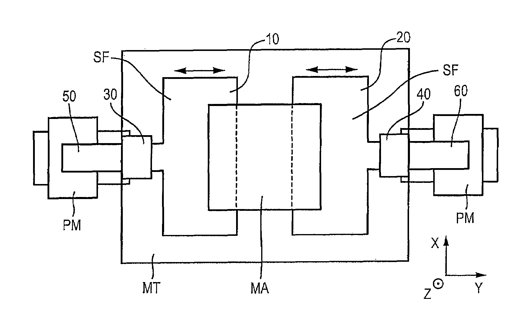
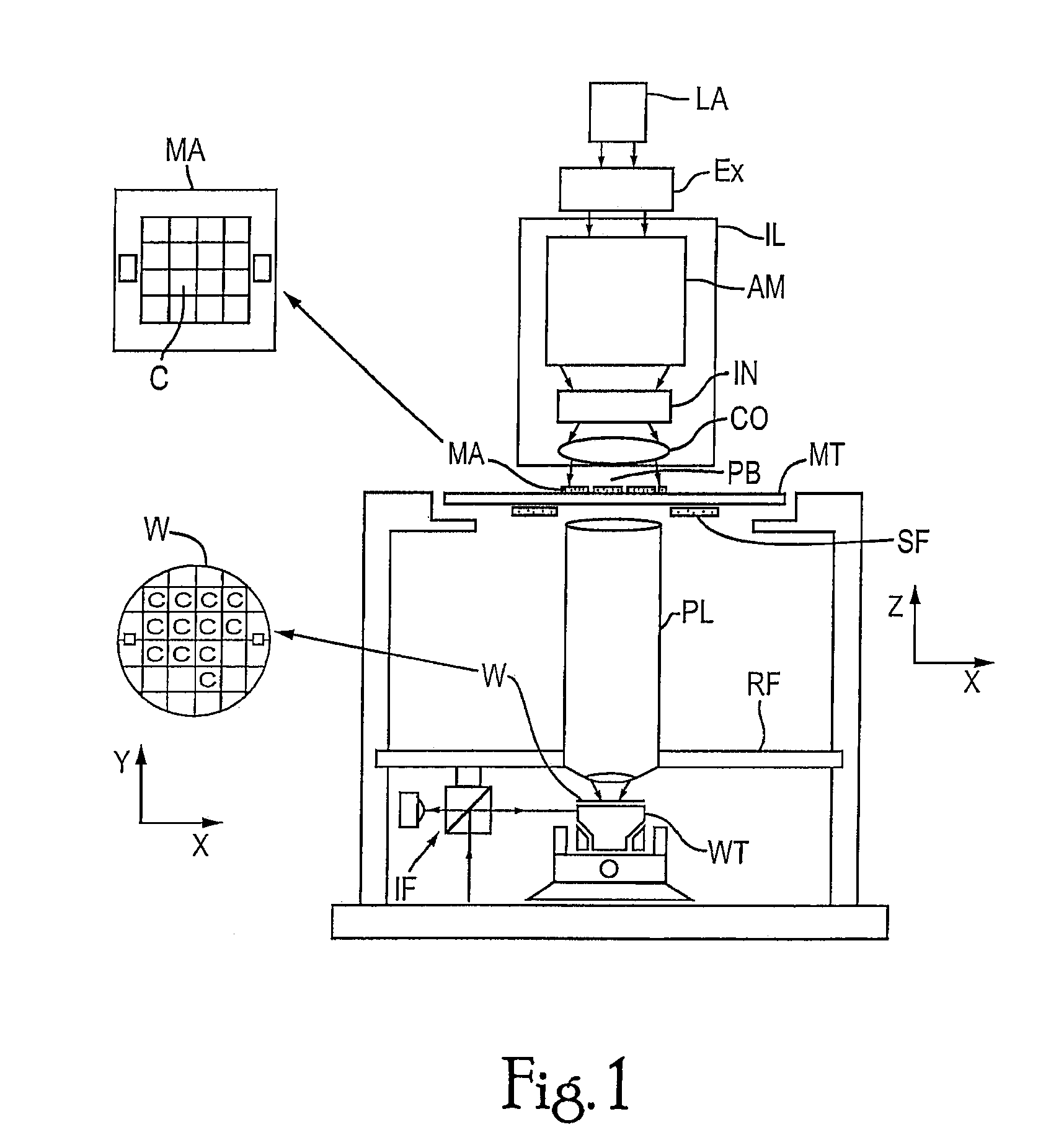
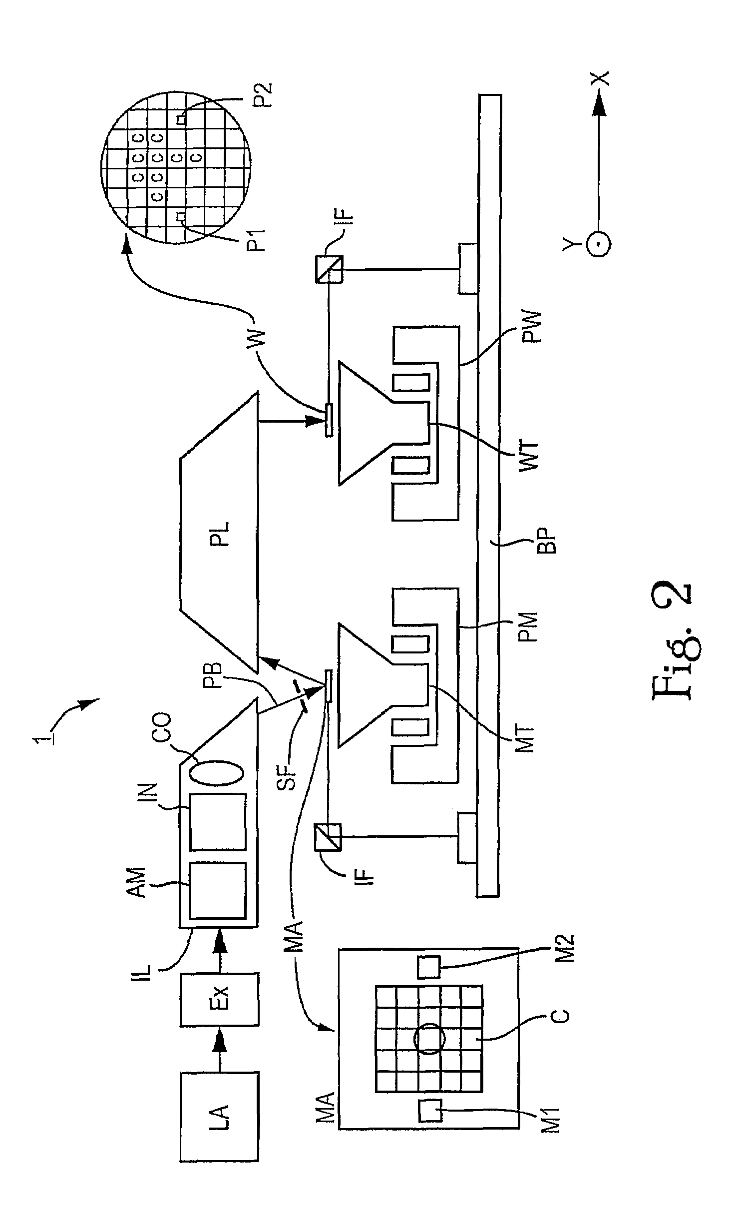
[0040]FIGS. 1 and 2 schematically depict a lithographic projection apparatus according to an embodiment of the invention. The apparatus comprises:[0041]an illumination system Ex, IL: for supplying a projection beam PB of radiation (e.g. EUV, DUV, or UV radiation). In this particular case, the radiation system also comprises a radiation source LA;[0042]a first object table (mask table / holder / holder) MT: provided with a mask holder for holding a mask MA (e.g. a reticle), and connected to first positioning mechanism for accurately positioning the mask with respect to item PL;[0043]a spatial filter SF: for example, a reticle masking device, also known in the art as a “rema” that is provided for selectively obstructing a part of the projection beam impinging on the mask or a part of the patterned beam;[0044]a second object table (substrate table / holder) WT: provided with a substrate holder for holding a substrate W (e.g. a resist-coated silicon wafer), and connected to second positioning...


PUM

PropertyMeasurementUnit
wavelengthaaaaaaaaaa

Abstract

A lithographic apparatus including means for selectively transmitting a projection beam before imaging the patterned projection beam onto a substrate. The means may include any of the following: a selectively transmitting device disposed downstream of a patterning device in the direction of the projection beam, a fixed and a moving set of masking blades in a scanning system or an array of switchable elements. The means may be provided to a mask table / holder or to a frame or structure of the lithographic projection apparatus.

Description

PRIORITY INFORMATION[0001]This application claims priority from European Patent Application No. 03076644.8, filed May 28, 2003, herein incorporated by reference in its entirety.BACKGROUND OF THE INVENTION[0002]1. Field of the Invention[0003]The present invention relates to a lithographic projection apparatus.[0004]2. Description of the Related Art[0005]Lithographic apparatus can be used, for example, in the manufacture of integrated circuits (ICs). In such a case, a patterning device may be used to generate a desired circuit pattern corresponding to an individual layer of the IC, and this pattern can be imaged onto a target portion (e.g. comprising one or more dies) on a substrate (silicon wafer) that has been coated with a layer of radiation-sensitive material (resist).[0006]The term “patterning device” as here employed should be broadly interpreted as referring to a device that can be used to impart an incoming radiation beam with a patterned cross-section, corresponding to a patt...

Claims


Application Information

Patent Timeline
Patent Type & Authority Patents(United States)
IPC IPC(8): G03B27/72G03F7/20H01L21/027
CPCG03F7/70191G03F7/70066
Inventor VAN SCHOTHORST, GERARDVAN DEUREN, FRANSISCUS HENDRIKUSVAN EIJK, JANLOOPSTRA, ERIK ROELOFMUNNIG SCHMIDT, ROBERT-HANPEETERS, FELIX GODFRIED PETER
Owner ASML NETHERLANDS BV
Learn More