SONOS memory array with improved read disturb characteristic

a memory array and read disturb technology, applied in the field of nonvolatile semiconductor memories, can solve the problems of even worse disturb problem, even more read disturb, and even more read disturb in the cells

Active Publication Date: 2008-09-09
ATMEL CORP
View PDF13 Cites 16 Cited by
  • Summary
  • Abstract
  • Description
  • Claims
  • Application Information

AI Technical Summary

Benefits of technology

[0006]In one example, in a SONOS memory transistor having the window described above, one of the two threshold voltages (a first threshold for transistor programming and a second threshold for transistor erasing) is kept flat while the read voltage is also flat in the window between the two threshold voltages. In a PMOS configuration, the threshold voltage for the erase state is the lowest voltage and is kept flat while holding the SONOS transistor voltage neutral for the erase state. In other words, the programmed and erased threshold levels of a SONOS cell can be chosen such that one of them is a neutral state in which there is no charge in the storage medium. For PMOS, it is advantageous that this state be the one with the lowest threshold, i.e., the erase threshold, since raising the threshold for programming the cell then requires the tunneling of electrons to the storage layer while lowering the threshold to the neutral state or erasing the cell would require the tunneling of holes to the storage layer which requires much higher voltages or longer times. This is because the barrier for injection of holes from the substrate through the tunnel oxide is higher and the effective mass of holes in silicon is higher. In this way the programming of the cell that needs to be done on a bit by bit basis can be done relatively quickly while erasing the cell which can be done for many bits at a time can be done more slowly in a flash memory array.
[0009]In a NAND memory, a second advantage for a PMOS cell is that the lowest threshold state will be the non-conducting state which must be overridden during read. Since this threshold is the one which is not subject to charge loss, the override voltage in a PMOS cell can be a fixed value with the smallest possible magnitude.

Problems solved by technology

A principal problem faced in memory arrays is read disturb, a situation where the read voltage applied to a cell disturbs the charge stored in the same cell or a nearby cell.
The problem of disturb is even worse in a NAND array in which a series of cells are places in a stack and a given cell must be read through the cells which are above it in the stack.
This requirement means that is such an array some cells will be subjected to even more read disturb.
Thus read disturb becomes an even bigger concern.

Method used


Image

  • SONOS memory array with improved read disturb characteristic
  • SONOS memory array with improved read disturb characteristic
  • SONOS memory array with improved read disturb characteristic

Examples


Embodiment Construction

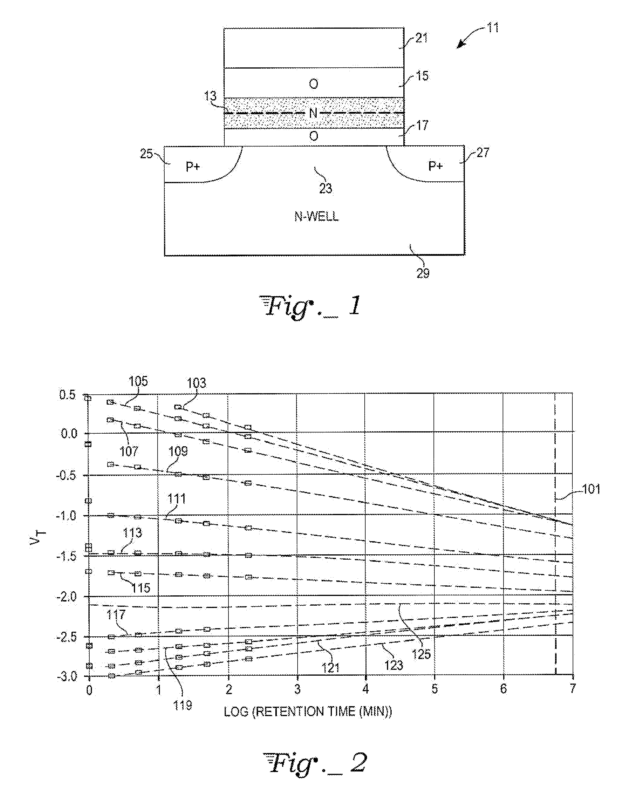
[0016]With reference to FIG. 1, a SONS non-volatile memory (NVM) cell 11 can be made by inserting a nitride trap storage layer 13 between the gate oxide layers 15, 17 to form a floating gate EEPROM transistor in the usual way. The top electrode 21 is usually conductive polysilicon. A channel 23 is formed between source 25 and drain 27 in N-well 29. Such a non-volatile memory cell 11 has advantages in terms of process simplicity and insensitivity to defects compared to more conventional floating gate cells due to the discrete nature of the trap storage locations within the nitride layer. The construction of such a cell has been widely discussed over the past several years. One method of programming and erasing such a cell consists of utilizing FN tunneling, modified FN tunneling, or direct tunneling by applying the appropriate biasing across the gate oxide layer 17. This method allows for low currents during programming which can be advantageous, especially in low power applications ...


PUM


Abstract

A PMOS non-volatile memory array using SONOS transistors having program and erase threshold voltages for representing digital logic states of zero and one and selected to optimize read disturb characteristics. The threshold voltages are linearly convergent and separated by at least 0.5 volts for a charge retention time of at least 10 years, with the threshold voltages defining a window wherein a read voltage for selected memory transistors can be held flat and not intersect the threshold voltages. The lower threshold is selected to be at a zero charge state for one of the two logic levels of the memory.

Description

TECHNICAL FIELD [0001]The invention relates to non-volatile semiconductor memories, and in particular to SONOS memories.BACKGROUND ART [0002]SONOS memory devices are electrically erasable programmable memory transistors wherein charge is stored in a nitride trap layer that is insulated from a substrate on one side and insulated from a select gate on another side. For example, such devices are described in “Characterization of Scaled SONOS EEPROM Memory Devices for Space and Military Systems” by M. White et al., IEEE 2004 p. 51-59. This paper describes device parameters, including retention time, in terms of various physical properties of devices. In NMOS SONOS cells an N-channel is formed in a P-well with the majority charge carriers being electrons. Charge is moved into nitride traps in the trap layer by various charge transfer mechanisms, such as hot electron transfer or Fowler-Nordheim (“FN”) tunnelling. Similarly, in PMOS SONOS cells a P-channel is formed in an N-well with the m...

Claims


Application Information

Patent Timeline
Patent Type & Authority Patents(United States)
IPC IPC(8): G11C11/34
CPCG11C16/3418G11C16/349G11C16/3427
Inventor PERLEGOS, GUSTRENNINGER, ALAN L.YOUNT, JAMESRYAN, MARIA
Owner ATMEL CORP
Why Eureka
Try Eureka