
Active matrix drive circuit

Active Publication Date: 2008-10-07
SOLAS OLED LTD +1
View PDF10 Cites 17 Cited by
  • Summary
  • Abstract
  • Description
  • Claims
  • Application Information

AI Technical Summary

Benefits of technology

[0007]Accordingly, it is an object of the present invention to provide an active matrix drive circuit which avoids the disadvantages of the prior art.
[0008]More particularly, it is an object of the present invention to provide an active matrix drive circuit with a current feedback, which requires less components and is simpler to manufacture than the known circuits.
[0011]The inventive circuit can be thereby always used when sufficiently homogenous LED parameter is provided. The inventive circuit has moreover the advantage that despite an additional thin film transistor, totally only three thin film transistors are required, since the non-linear LED characteristic is used for switching off of the current through the LED element. In other words, no separate switch must be provided for the current. This also makes possible the realization of all circuit parts at one side of the LED element, so that a conventional layer sequence can be used during the manufacture. A through contacting through the LED material, in particular through the organic material with an organic LED, is not necessary.
[0012]The gate electrode of the third transistor can be connected with the scanning signal conductor, so that the third transistor is activated together with the second transistor, when the image point is selected. This saves the otherwise required additional driving conductor.
[0013]Further advantages are provided in accordance with the present invention when the components of the current measuring- and voltage regulating circuit connected with the split conductors are low-ohmic, so that total very short response times are provided.

Problems solved by technology

Thereby disturbing spacial inhomogenuities of the image screen light density are caused.
These circuits provide however only a partial compensation and therefore, with a great number of transistors, produced a relatively low manufacturing yield.
The current-controlled solutions are very high-ohmic and require relatively long response times. With the use of pure current mirror circuits, two thin filmed transistors must have approximately identical properties, that is difficult to implement for thin filmed transistors.
A further disadvantage of the known, above described current feedback circuit is that parts of the drive circuit must be realized at both sides of the LED element, that requires a technically extremely difficult-to-produce through contacting with the LED semiconductor material; in particular with organic semiconductor materials.
Moreover, the known circuit is expensive since four additional thin filmed transistors are required, including two thin film transistors which act as switches and two thin film transistors for an invertor.

Method used


Image

  • Active matrix drive circuit
  • Active matrix drive circuit

Examples


Embodiment Construction

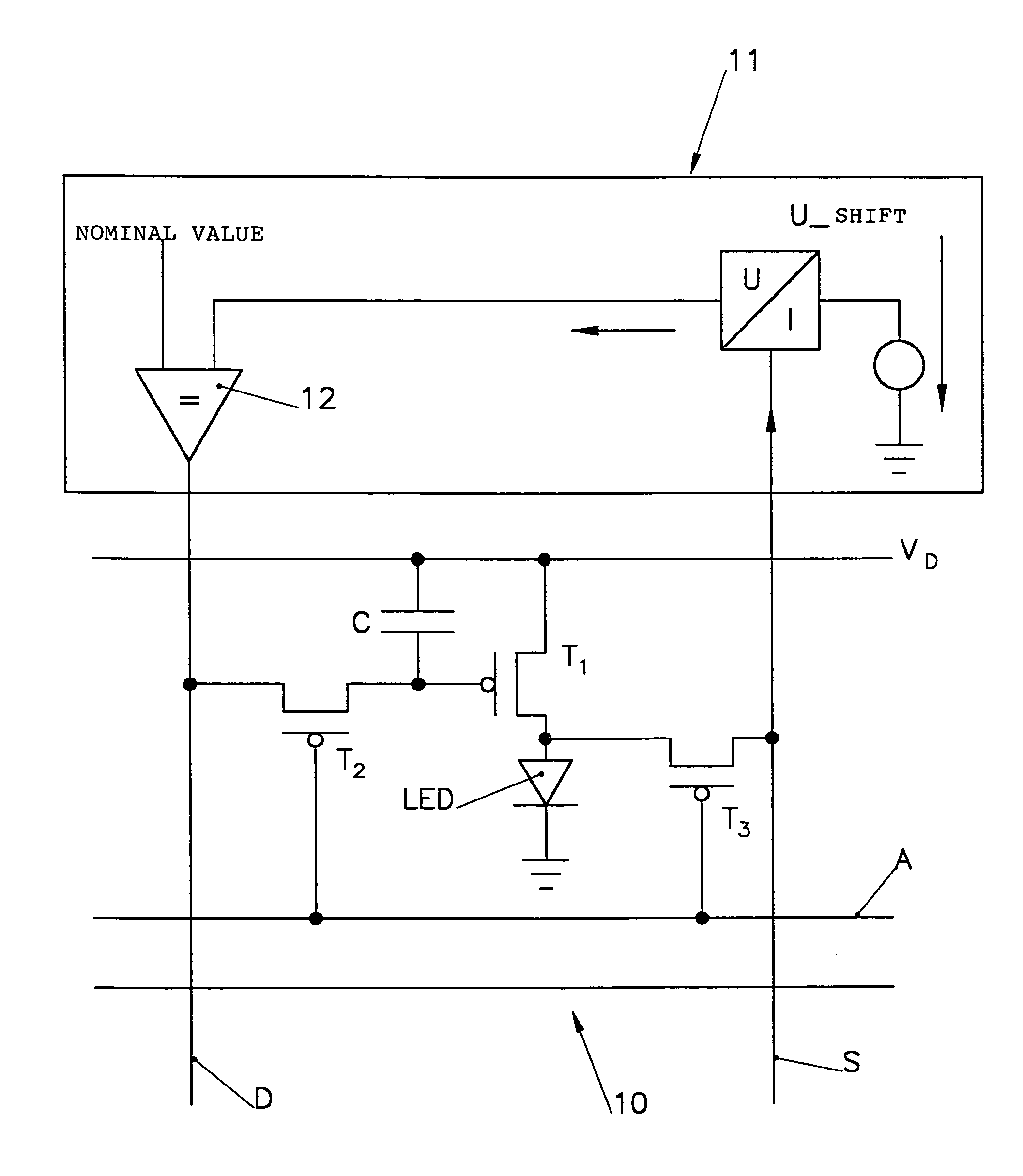
[0016]The single FIGURE of the drawings is a view showing a switching diagram of a typical drive circuit in accordance with the present invention, with P-channel-TFTs (T1, T2) for an image point 10 of a display. Naturally, also corresponding layouts with N-channel-TFTs or CMOS implementations are possible. The image point 10 has an organic, light-emitting diode LED with a cathode connected to ground.

[0017]A first thin film transistor T1 acts as a current-driving transistor for the LED element. The transistor T1 is driven by a second thin film transistor T2. The second thin film transistor T2 is connected with its drain-terminal with a data conductor D and with its source-terminal with the gate of the first thin film transistor T1. The gate of the second thin film transistor T2 is connected with a scanning signal conductor A. Moreover, the driving circuit has a first capacitor C. It is arranged between the supply voltage VD and the gate of the current driving transistor T1 and serves...


PUM


Abstract

A driving circuit for an image point of an image screen which has an organic light-emitting diode includes a capacitor, a feedback coupling, a first thin film transistor as a current-driving transistor for the diode, a second transistor which is connected by a current-conducting electrode with a gate of the first transistor and by a second current-conducting electrode with a data conductor and by its gate electrode with a scanning signal conductor, a third thin film transistor which during driving its gate through a driving conductor taps a diode driving current and an output of the first transistor and supplies a current measuring- and voltage regulating circuit, the current measuring- and voltage regulating circuit providing to the data conductor a voltage signal which is dependent on a current measuring result and a voltage comparison, so that the diode during driving of the gate of the third transistor due to its non-linear switching characteristic acts as a switch for a current deviation in the current measuring- and voltage regulating circuit.

Description

BACKGROUND OF THE INVENTION[0001]The present invention relates to a drive circuit for an image point of an image screen, which has in particular an organic light-emitting diode, with a capacitor and a current feedback, wherein a first thin film transistor is provided as the current driving transistor for the diode, and a second thin film transistor is connected with a current-conducting electrode with a gate of the first transistor and with a second current-conducting electrode with a data conductor and with its gate electrode with a scanning signal conductor.[0002]In the driving of image screens with light-emitting diodes (LED), in particular organic, light-emitting diodes (OLED) via thin film transistors, spacial fluctuations of the LED driver currents occur because of manufacturing-dependent fluctuations of the parameters of the thin film transistors, in particular the threshold voltage and the charge carrier movement. Thereby disturbing spacial inhomogenuities of the image scree...

Claims


Application Information

Patent Timeline
IPC IPC(8): G09G3/32G09F9/30H01L51/50G09F9/33G09G3/20G09G3/30
CPCG09G3/3233G09G2300/043G09G2300/0842G09G2320/043G09G2320/029G09G2320/0295G09G2320/0233G09G3/30
Inventor FRUEHAUF, NORBERT
Owner SOLAS OLED LTD
Features
  • Generate Ideas
  • Intellectual Property
  • Life Sciences
  • Materials
  • Tech Scout
  • Unparalleled Data Quality
  • Higher Quality Content
  • 60% Fewer Hallucinations
Learn More