Electroluminescence device, manufacturing method thereof, and electronic apparatus

a manufacturing method and technology of electroluminescent devices, applied in the direction of electroluminescent light sources, solid-state devices, electric lighting sources, etc., can solve the problems of reducing the ability of capacitors to be formed, and generating considerable parasitic capacitance between the conductive substrate and the wiring, so as to increase the storage capacitance, and reduce the parasitic capacitance

Inactive Publication Date: 2008-10-14
SEIKO EPSON CORP
View PDF4 Cites 39 Cited by
  • Summary
  • Abstract
  • Description
  • Claims
  • Application Information

AI Technical Summary

Benefits of technology

[0007]An advantage of the invention is to provide: an organic EL device that satisfies both requirements of increasing the storage capacitance and decreasing the parasitic capacitance; and a manufacturing method of the organic EL device.
[0008]According to a first aspect of the invention, an organic electroluminescence device includes: a substrate having conductivity on at least one side; a first insulation film, formed on one side of the substrate, while having an aperture which partially exposes the same side of the substrate; a semiconductor film, formed on the first insulation film, while covering a part of the first insulation film; a second insulation film formed on the first insulation film, while covering the semiconductor film and contacting the same side of the substrate via the aperture; a capacitor electrode, formed on the aperture, while sandwiching the second insulation film so as to face the substrate; a gate electrode formed on the semiconductor film, so as to sandwich the second insulation film; and an organic electroluminescence element, formed on the second insulation film, electrically connected to the semiconductor film.
[0009]According to a second aspect of the invention, an organic electroluminescence device includes: a substrate having conductivity on at least one side; a first insulation film, formed on one side of the substrate, while having an aperture which partially exposes the same side of the substrate; a gate electrode, formed on the first insulation film, while covering a part of the first insulation film; a second insulation film formed on the first insulation film, while covering the gate electrode and contacting the same side of the substrate via the aperture; a capacitor electrode, formed on the aperture, while sandwiching the second insulation film so as to face the substrate; a semiconductor film formed on the gate electrode, so as to sandwich the second insulation film; and an organic electroluminescence element, formed on the second insulation film, electrically connected to the semiconductor film.
[0010]According to the above aspects of the invention, combining the first insulation film and the second insulation film allows a separation of functions required in insulation films. In other words, conditions such as film thickness or permittivity, suitable for reducing the parasitic capacitance, can be set for the first insulation film, while assuring the insulation between the substrate and the organic electroluminescence elements or the transistors installed on this substrate. Moreover, conditions such as film thickness or permittivity, suitable for increasing an electrostatic capacitance, can be set for the second insulation film, when forming capacitive elements being sandwiched by the conductive substrate and the capacitor electrode. Consequently, the increase of the storage capacitance increase of the capacitive elements, and the decrease of the parasitic capacitance generated between the substrate and the circuit component, are simultaneously obtained.
[0011]In the above aspects, it is preferable that the film thickness of the second insulation film be smaller than that of the first insulation film. Moreover, it is preferable that the permittivity of the second insulation film be larger than that of the first insulation film.
[0012]This allows an increase of the electrostatic capacitance of the capacitive element, while adequately assuring the insulating property between the conductive substrate and at least one of the transistor and the organic EL element.

Problems solved by technology

However, the region in which the capacitor can be formed is limited to the area surrounded by the scanning line (gate wiring) and the signal line (source wirings).
On the other hand, a considerable parasitic capacitance is generated between the conductive substrate and the wirings when the thickness of the insulation film is small.
Consequently, fulfilling the two contradicting requirements, which is to increase the storage capacitance and to decrease the parasitic capacitance, is difficult.

Method used


Image

  • Electroluminescence device, manufacturing method thereof, and electronic apparatus
  • Electroluminescence device, manufacturing method thereof, and electronic apparatus
  • Electroluminescence device, manufacturing method thereof, and electronic apparatus

Examples


Embodiment Construction

[0040]Embodiments of the present invention will now be described.

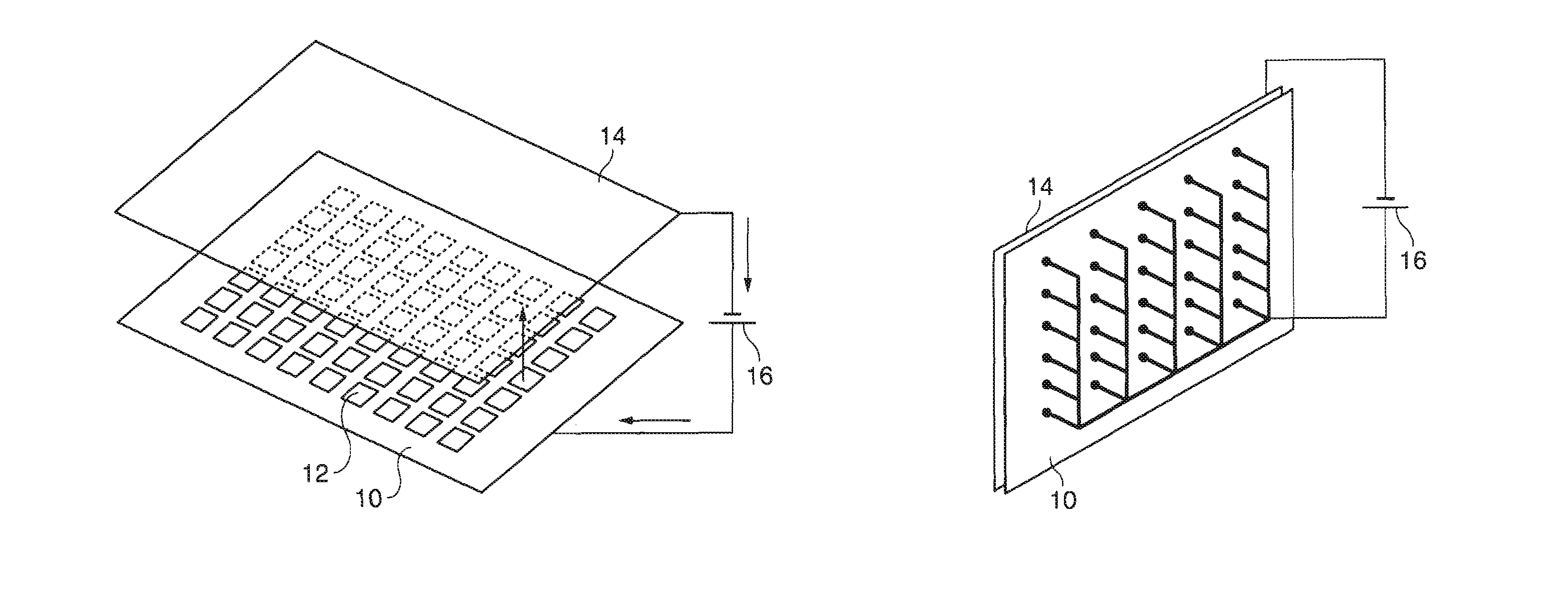
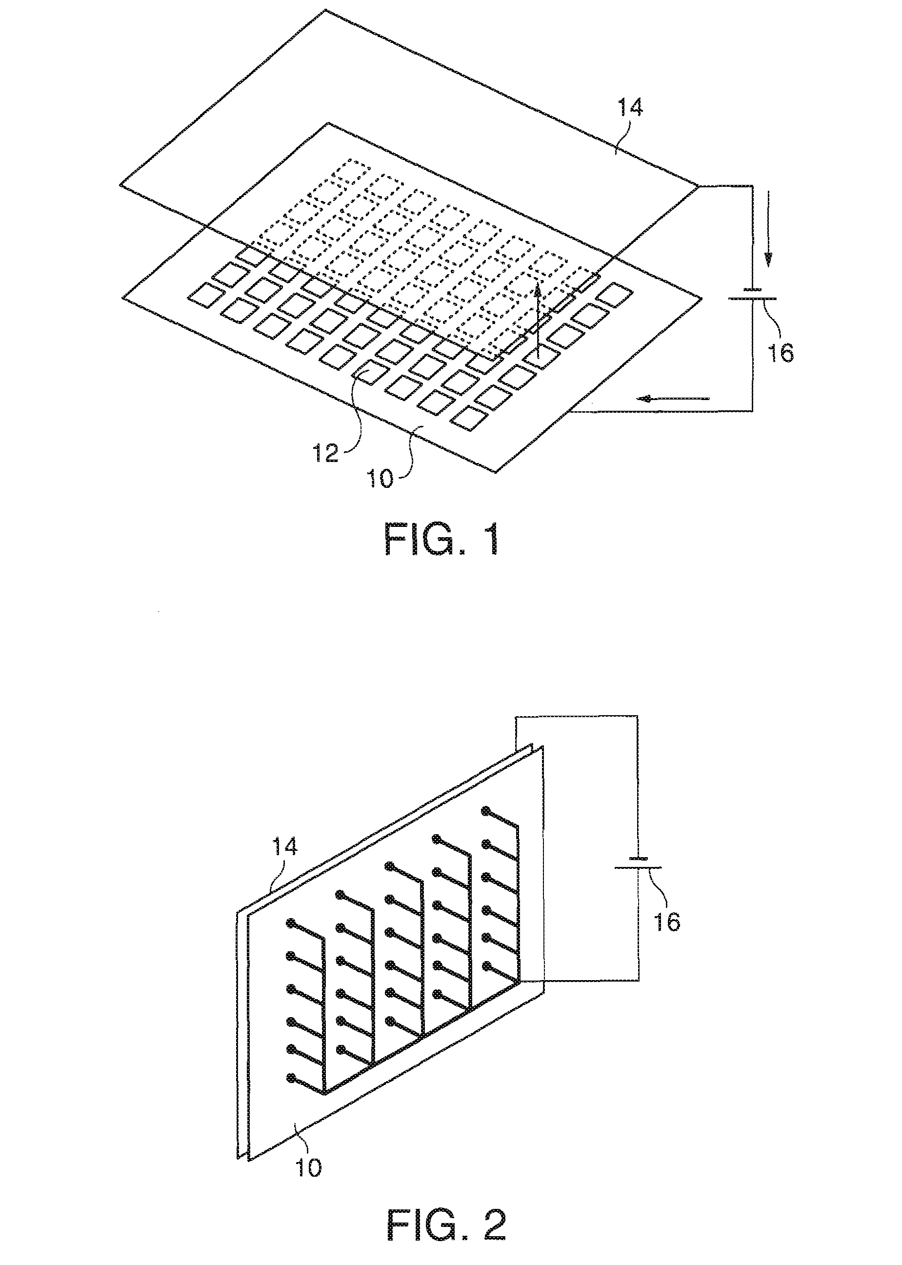
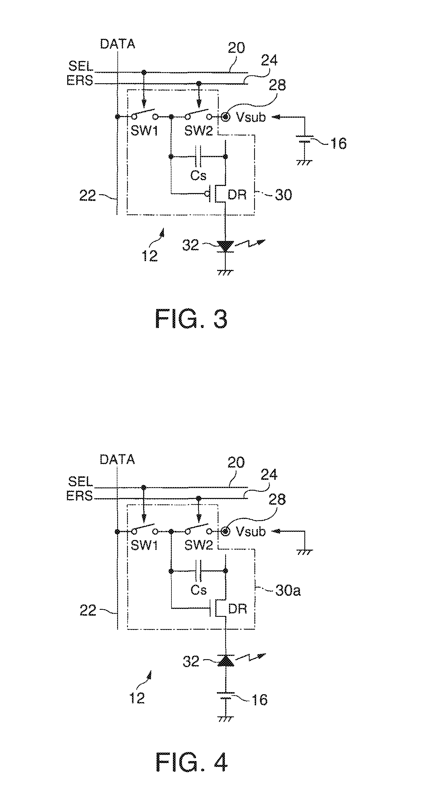
[0041]FIG. 1 is a schematic drawing describing a basic structure of an organic EL device according to each of the embodiments. The organic EL device includes: a substrate 10 having conductivity; a plurality of pixel units 12 formed on one side of the substrate 10; and a common electrode 14 shared by the plurality of pixel units 12. As shown in FIG. 1, a power source 16 is connected between the substrate 10 and the common electrode 14.

[0042]As long as conductivity is provided to at least one side of the substrate 10, the substrate 10 may be an insulating substrate, while it is preferable that the substrate 10 be a conductive substrate composed with conductors. Examples of the substrate 10 for the former option above include the ones where a conductive film composed of metals such as aluminum or of indium tin oxide (ITO) is deposited on one side of the insulating substrates such as a glass, a quartz, and ceramic substrat...


PUM


Abstract

An organic electroluminescence device including: a substrate having conductivity on at least one side; a first insulation film, formed on one side of the substrate, while having an aperture which partially exposes the same side of the substrate; a semiconductor film, formed on the first insulation film, while covering a part of the first insulation film; a second insulation film formed on the first insulation film, while covering the semiconductor film and contacting the same side of the substrate via the aperture; a capacitor electrode, formed on the aperture, while sandwiching the second insulation film so as to face the substrate; a gate electrode formed on the semiconductor film, so as to sandwich the second insulation film; and an organic electroluminescence element, formed on the second insulation film, electrically connected to the semiconductor film.

Description

BACKGROUND[0001]1. Technical Field[0002]Several aspects of the present invention relate to an organic electroluminescence device having a plurality of organic electroluminescence (hereafter referred to as “EL”) elements formed on a substrate, the manufacturing method thereof, and an electronic apparatus including the organic EL device.[0003]2. Related Art[0004]The organic EL device includes, as its main components a circuit element substrate and organic EL elements. This circuit element substrate includes a substrate such as glass substrates, wirings formed thereon, and pixel circuits connected to those wirings. Those wirings include, for instance, a plurality of scanning lines, and a plurality of signal lines and power lines that are aligned to cross these scanning lines. Here, the power lines supply electric power to the organic EL elements. The pixel circuits are arranged at the crossing points of the scanning lines and the signal lines. Each pixel circuit functions in a manner t...

Claims


Application Information

Patent Timeline
Patent Type & Authority Patents(United States)
IPC IPC(8): H01L21/00
CPCH01L27/3244H01L27/3265H10K59/1216H10K59/12H05B33/22H05B33/02
Inventor TODOROKIHARA, MASAYOSHIMIYASHITA, KAZUYUKI
Owner SEIKO EPSON CORP
Why Eureka
Try Eureka