Shift register circuit and image display apparatus containing the same

a register circuit and image display technology, applied in logic circuits, digital storage, instruments, etc., can solve problems such as gate lines being activated, affecting the drive capability of the second transistor, and unable to pass curren

Inactive Publication Date: 2008-10-14
TRIVALE TECH LLC
View PDF24 Cites 143 Cited by
  • Summary
  • Abstract
  • Description
  • Claims
  • Application Information

AI Technical Summary

Benefits of technology

[0025]Threshold voltage shifts of transistors which are constituents of a shift register circuit are controlled to prevent a malfunction in the shift register circuit.
[0028]In a conventional shift register circuit with only one pull-down circuit that discharges a first node during a period when the first node is not charged (a non-selected period), since a specific transistor in that pull-down circuit needs to continuously discharge the first node, the control electrode of that transistor is continuously biased, which causes a threshold voltage shift of the transistor. According to the present invention, the first pull-down circuit and the second pull-down circuit operate such that they discharge the first node in turn during the non-selected period, so that it is not necessary to continuously bias the control electrode of a specific transistor in those pull-down circuits. This reduces deterioration in the drive capabilities of the first and the second pull-down circuits and allows the first node to be discharged with reliability, thereby preventing a malfunction in the shift register circuit.

Problems solved by technology

But, a-Si TFTs have a tendency that, when their gate electrodes are positively and continuously (dc) biased, their threshold voltages may shift in a positive direction, which causes impaired drive capabilities (capabilities to pass current).
Repeating that operation impairs the drive capability of the second transistor.
If that is the case, when unnecessary charges are supplied to the output terminal due to noise or the like, the second transistor cannot discharge those charges and such a malfunction results that the gate lines may be activated by mistake.
It is known that a similar problem can occur not only in a-Si TFTs but also in, for example, organic TFTs.
Doing so, however, causes the following problem.
Consequently, there is concern that the level of the gate of the first transistor (Tu) might rise during the non-selected period.
The problem is that if, at this time, the level of the gate exceeds the threshold voltage of the first transistor (Tu), an error output signal will be outputted.

Method used


Image

  • Shift register circuit and image display apparatus containing the same
  • Shift register circuit and image display apparatus containing the same
  • Shift register circuit and image display apparatus containing the same

Examples


first preferred embodiment

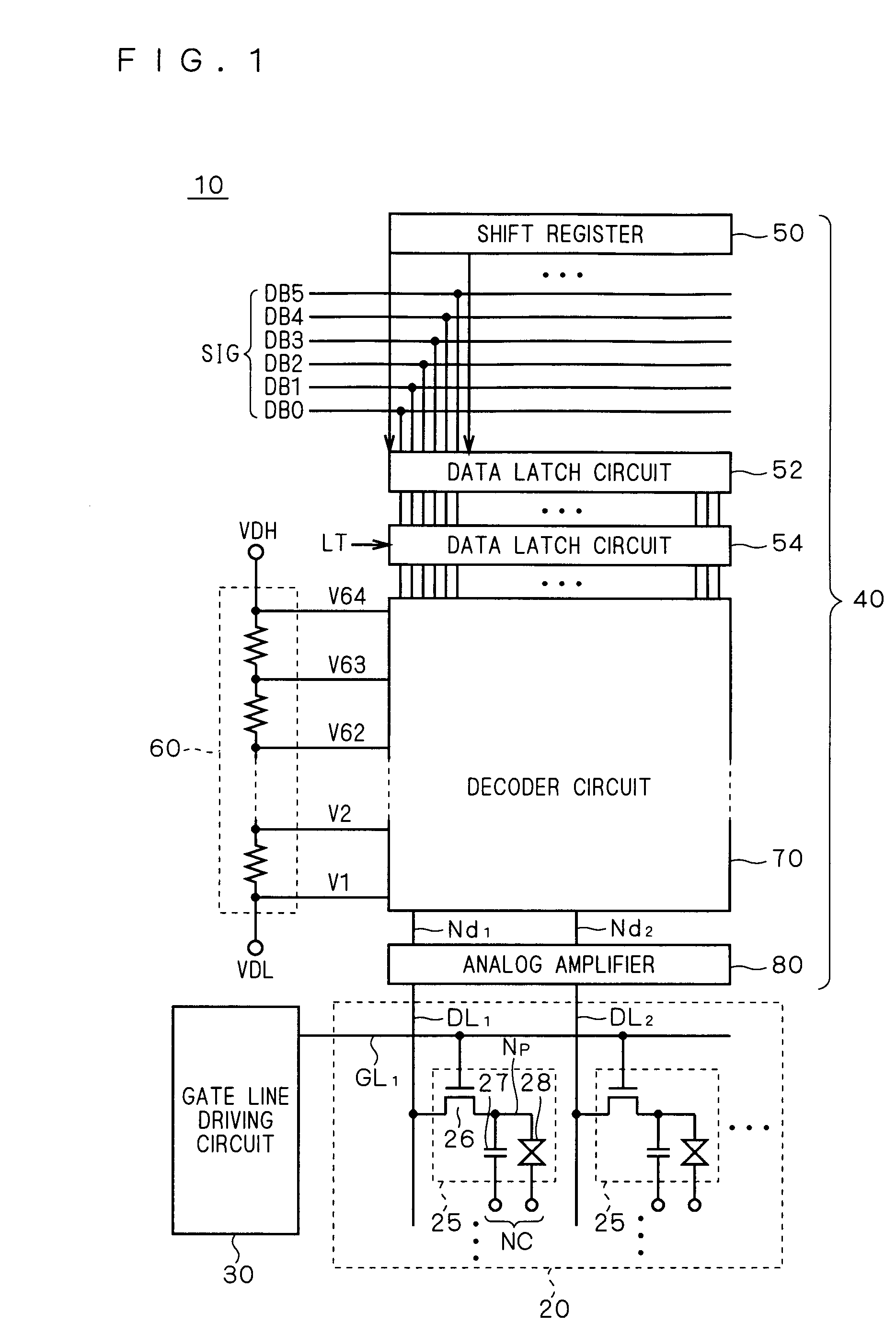
[0064]FIG. 1 is a schematic block diagram showing a configuration of a display apparatus according to a first preferred embodiment of the present invention. It shows an overall configuration of a liquid crystal display 10 as a representative example of the display apparatus.

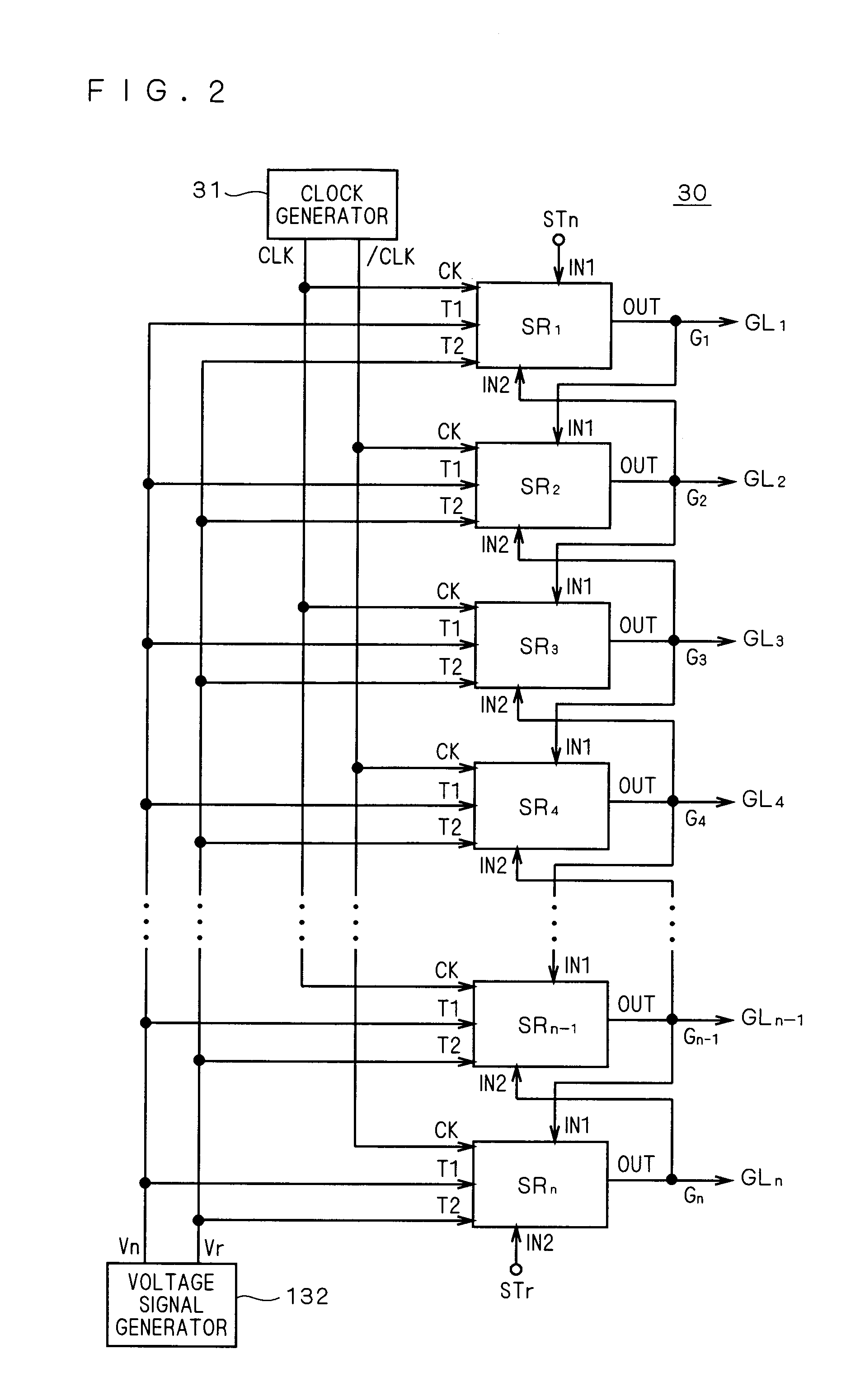
[0065]The liquid crystal display 10 includes a liquid crystal array 20, a gate line driving circuit (scanning line driving circuit) 30, and a source driver 40. As will be clear from the following description, a bidirectional shift register according to the preferred embodiments of the present invention is mounted in the gate line driving circuit 30 and is formed integrally with the liquid crystal array 20.

[0066]The liquid crystal array 20 includes a plurality of pixels 25 arranged in a matrix. Each of gate lines GL1, GL2, . . . (hereinafter also referred to generically as “gate lines GL”) is provided for each row of pixels (hereinafter also referred to as a “pixel line”), and each of data lines DL1, DL2, . . . (h...

second preferred embodiment

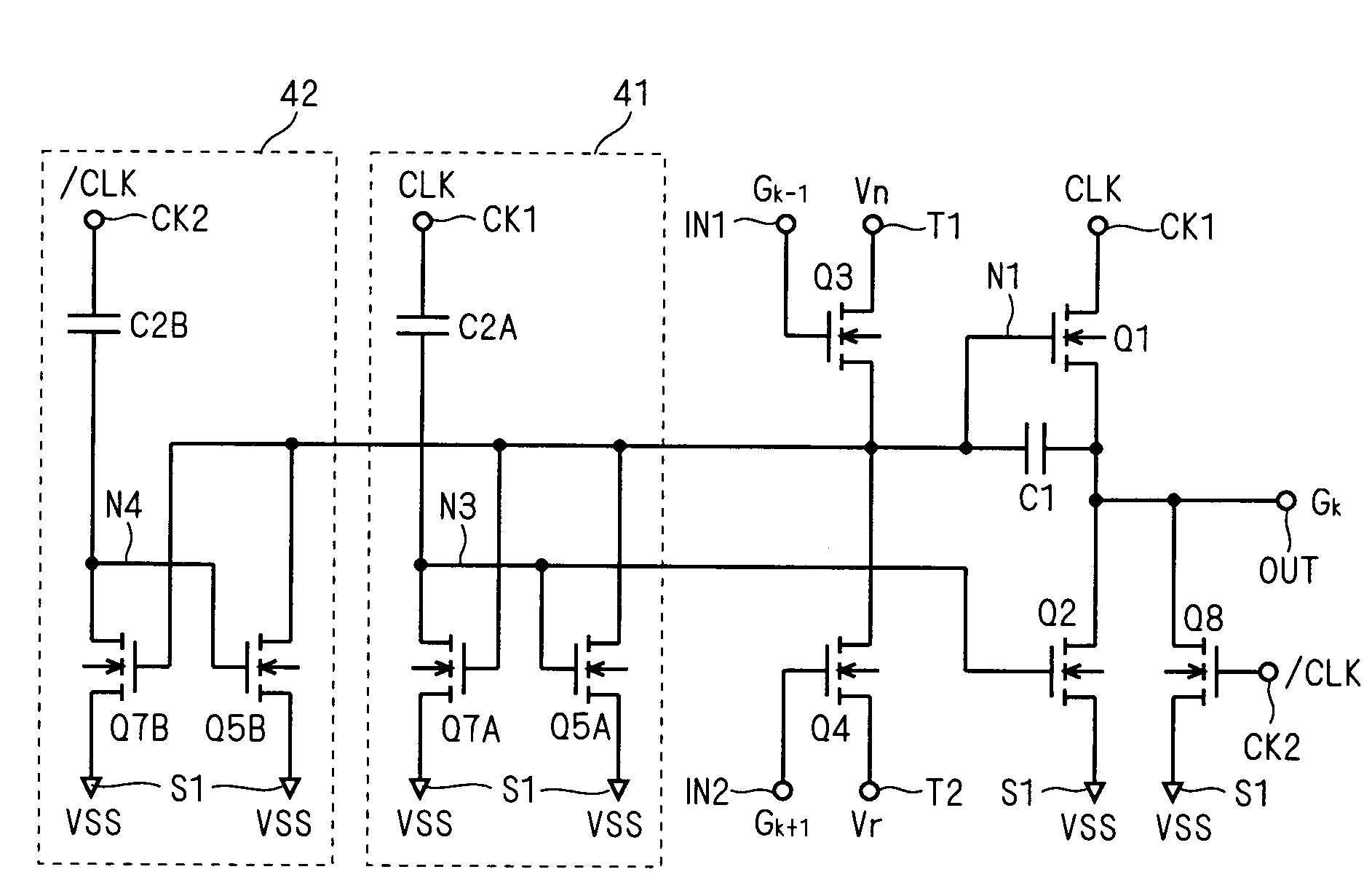
[0165]Hereinbelow, variations of the first pull-down circuit 41 and the second pull-down circuit 42 in the unit shift register SR according to the present invention will be described. As will be described later, as to the first pull-down circuit 41, the one described in the first preferred embodiment (FIG. 8) is basically preferable. Thus, the following description is mainly related to the details of variations of the second pull-down circuit 42.

[0166]FIG. 11A is a circuit diagram of the second pull-down circuit 42 according to a second preferred embodiment. FIG. 11A shows an example that the clock signal CLK is inputted to the first clock terminal CK1 and the clock signal / CLK is inputted to the second clock terminal CK2 (the same applies to each circuit diagram of FIG. 12 and following drawings).

[0167]According to this preferred embodiment, in contrast to the second pull-down circuit 42 of FIG. 8, the capacitive element C2B is replaced by transistors Q6B and Q9B. The transistor Q6...

third preferred embodiment

[0177]FIG. 12A is a circuit diagram of the second pull-down circuit 42 according to a third preferred embodiment. According to this preferred embodiment, in contrast to the circuit of FIG. 11A, the transistor Q7B is replaced by two transistors Q7Bn and Q7Br. The transistor Q7Bn is connected between the node N4 and the first power supply terminal S1 so that its gate is connected to the first input terminal IN1. The transistor Q7Br is connected between the node N4 and the first power supply terminal S1 so that its gate is connected to the second input terminal IN2

[0178]The on-resistance of the transistor Q6B is set sufficiently higher than those of the transistors Q7Bn and Q7Br so that a pair of the transistors Q6B and Q7Bn and a pair of the transistors Q6B and Q7Br each form a ratio inverter. In other words, the on-resistances of the transistors Q7Bn and Q7Br are set sufficiently lower then that of the transistor Q6B. Thus, assuming that the second clock terminal CK2 is at the HIGH l...


PUM


Abstract

Threshold voltage shifts of transistors which are constituents of a bidirectional shift register are reduced to prevent a malfunction in the shift register. A bidirectional unit shift register includes first and second pull-down circuits (41, 42) connected to the gate of a first transistor (Q1) that supplies a first clock signal (CLK) to an output terminal (OUT). The first pull-down circuit (41) includes a first inverter that uses the gate of the first transistor (Q1) as the input node and that is activated by the first clock signal (CLK), and a second transistor (Q5A) that discharges the gate of the first transistor (Q1) according to the output of the first inverter. The second pull-down circuit (42) includes a second inverter that uses the gate of the first transistor (Q1) as the input node and that is activated by a second clock signal ( / CLK) having a different phase from the first clock signal (CLK), and a third transistor (Q5A) that discharges the gate of the first transistor according to the output of the second inverter.

Description

BACKGROUND OF THE INVENTION[0001]1. Field of the Invention[0002]The present invention relates to a shift register circuit for use as, for example, a scanning line driving circuit in an image display apparatus and constituted by only field-effect transistors of the same conductivity type, and in particular to a bidirectional shift register that can reverse the direction of shift of a signal.[0003]2. Description of the Background Art[0004]In an image display apparatus (hereinafter referred to as a “display apparatus”) such as a liquid crystal display, a plurality of pixels are arranged in a matrix in a display panel and a gate line (scanning line) is provided for each row of pixels (pixel line) of the display panel. In a cycle of one horizontal period of a display signal, the gate lines are sequentially selected and driven to update a display image. As a gate line driving circuit (scanning line driving circuit) for sequentially selecting and driving pixel lines, i.e., gate lines, a sh...

Claims


Application Information

Patent Timeline
Patent Type & Authority Patents(United States)
IPC IPC(8): G11C19/00
CPCG09G3/3677G11C19/184G11C19/28H03K19/096G09G2300/0417G09G2310/0283G09G2310/0286G09G3/20G09G3/36G11C19/00H03K19/00
Inventor TOBITA, YOUICHI
Owner TRIVALE TECH LLC
Why Eureka
Try Eureka