Photoelectric conversion apparatus and photoelectric conversion system having the apparatus

a conversion system and photoelectric technology, applied in the field of photoelectric conversion apparatus and photoelectric conversion system having the apparatus, can solve the problems of imposing a large load on the patient, affecting the efficiency of diagnosis and treatment, and requiring a lot of time for the x-ray image pickup apparatus of the conventional film method, so as to reduce the read scanning time, reduce the generation of thermal noise, and improve the effect of image information

Inactive Publication Date: 2008-10-21
CANON KK
View PDF26 Cites 9 Cited by
  • Summary
  • Abstract
  • Description
  • Claims
  • Application Information

AI Technical Summary

Benefits of technology

[0030]An object of the present invention is to provide a photoelectric conversion apparatus that can reduce the read scanning time so as to enable high-speed reading and also to provide a system having the apparatus.
[0031]Another object of the present invention is to provide a photoelectric conversion apparatus that can perform signal reading at high S / N with little generation of thermal noise (KTC noise) and also to provide a system having the apparatus.
[0032]An additional object of the present invention is to provide a photoelectric conversion apparatus that can obtain good image information without density unevenness or unnecessary stripes, reduced in fixed pattern noise, and also to provide a system having the apparatus.
[0033]A further object of the present invention is to provide a photoelectric conversion apparatus that can obtain image information excellent in tone level and also to provide a system having the apparatus.
[0034]Still another object of the present invention is to provide a photoelectric conversion apparatus that can be corrected readily for nonuniformity of characteristic such as one caused by manufacturing dispersion of photoelectric conversion element or the like, thereby enabling further promotion of cost reduction and also to provide a system having the apparatus.

Problems solved by technology

Even under such circumstances, the X-ray image pickup apparatus of the conventional film method requires a lot of time because of intervention of a development step of film before a doctor obtains a patient's X-ray image.
These are factors to impede an improvement in the efficiency of diagnosis and treatment in hospitals and also force a great load on the patient, which would be great hindrance against development to new medical society in future.
In the non-destructive examination typified by examination of the inside of an object such as a building body, it is not permissible to repeat setting of various devices for X-ray photography or to repeat photography of necessary parts, either.
In the case of the film method, however, whether photography of necessary parts is completed cannot be found before the end of development in such examination, either.
Since expert's judgment is made after completion of development of film, it is not possible for the expert to give an instruction of photography at another in situ angle or an instruction of treatment in situ when necessary.
However, in the photoelectric conversion apparatus for successively performing the operations of from transfer through reading to reset, even with employing such structure, the time necessary for reading pixels in one line (=4000 / N pixels) needs to include the transfer time T1 and reset time T2 every time of reading the pixels in each line, and therefore, the apparatus has a problem that the scanning time of photoelectric conversion, especially, with a lot of pixels was sometimes longer than expected.
Also, there is a possibility of raising a problem that upon performing the transfer operation from the load capacitor (C1 to C3) to the operational amp OP side through the switching element (U1 to U3) controlled by the shift register SR2, the thermal noise occurring due to thermal agitation of carriers in the switching elements might degrade S / N of the photoelectric conversion apparatus in some cases.
Similarly, the KTC noise also occurs upon resetting the load capacitances to the reset potential by the reset switches RES1 to RES3, which raises the problem of reduction in S / N of the photoelectric conversion apparatus.
Especially, if high-definition and high-gradation-level information is desired to obtain as in the medical X-ray image pickup apparatus, the apparatus will necessitate the photoelectric conversion apparatus with higher S / N ratios than the business machines such as copiers or electronic blackboards, and, the KTC noise could be a big problem.
When the switching elements having the interelectrode capacitance Cgs are made of an a-Si semiconductor thin film, individual differences will appear in capacitance values of load capacitance CL among apparatus because of dispersion in film thickness on fabrication of thin film, which would raise a problem that apparatus with high output and apparatus with low output are manufactured.
In order to overcome it, upon constructing the system, such a countermeasure is taken as to add a general-purpose OP amp to adjust the gain, but the above example necessitates N general-purpose amplifiers, which will raise the cost of apparatus when also taking the adjustment process into consideration.
However, if many (N) ICs are provided, heat generation thereof will increase the temperature of the photoelectric conversion circuit section in some cases.
Especially, when the switching elements are amorphous silicon TFTs, it is said that the dark current during OFF will increase, and there is a possibility of raising another problem that the heat generation of ICs could increase fixed pattern noise of photoelectric conversion apparatus.

Method used


Image

  • Photoelectric conversion apparatus and photoelectric conversion system having the apparatus
  • Photoelectric conversion apparatus and photoelectric conversion system having the apparatus
  • Photoelectric conversion apparatus and photoelectric conversion system having the apparatus

Examples


embodiment 1

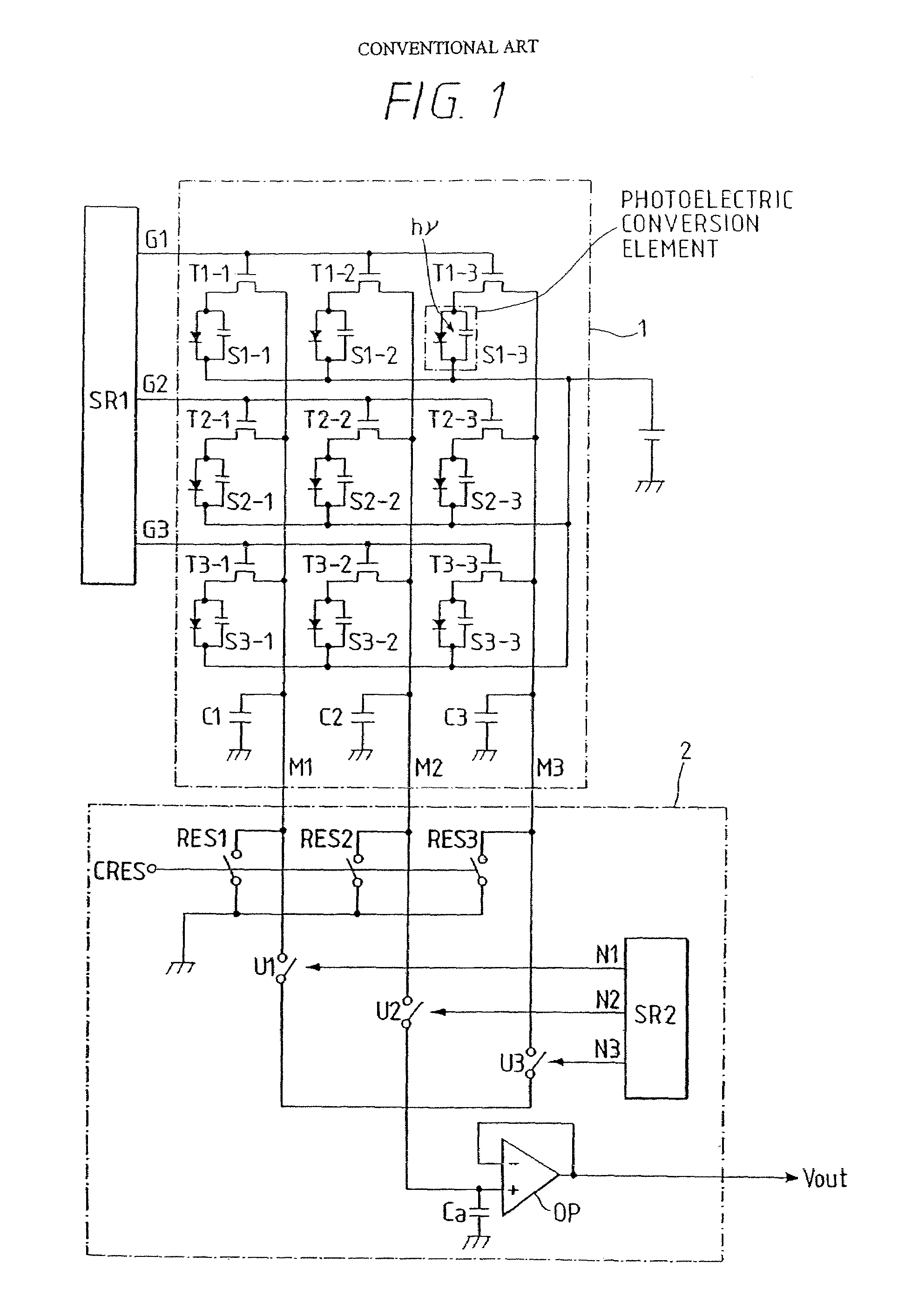
[0095]FIG. 3 is a circuit diagram of a photoelectric conversion apparatus to show the first embodiment of the present invention. For simplifying the description, the figure illustrates the structure of 3×3, nine pixels in total. Further, the same members as those in FIG. 1 will be denoted by the same symbols. S1-1 to S3-3 are photoelectric conversion elements for receiving the visible light and converting it to electric signals, and T1-1 to T3-3 are switch elements for transferring signal charges obtained by photoelectric conversion in the photoelectric conversion elements S1-1 to S3-3 to the matrix signal wires M1 to M3. G1 to G3 represent wires for driving the gates of switches, connected to the shift register (SR1) and connected to the switch elements T1-1 to T3-3. The capacitance comprised of three interelectrode capacitances (Cgs) of switch elements is applied to the matrix signal wire M1 upon transfer, as described above, and it is not illustrated as a capacitor element in FIG...

embodiment 2

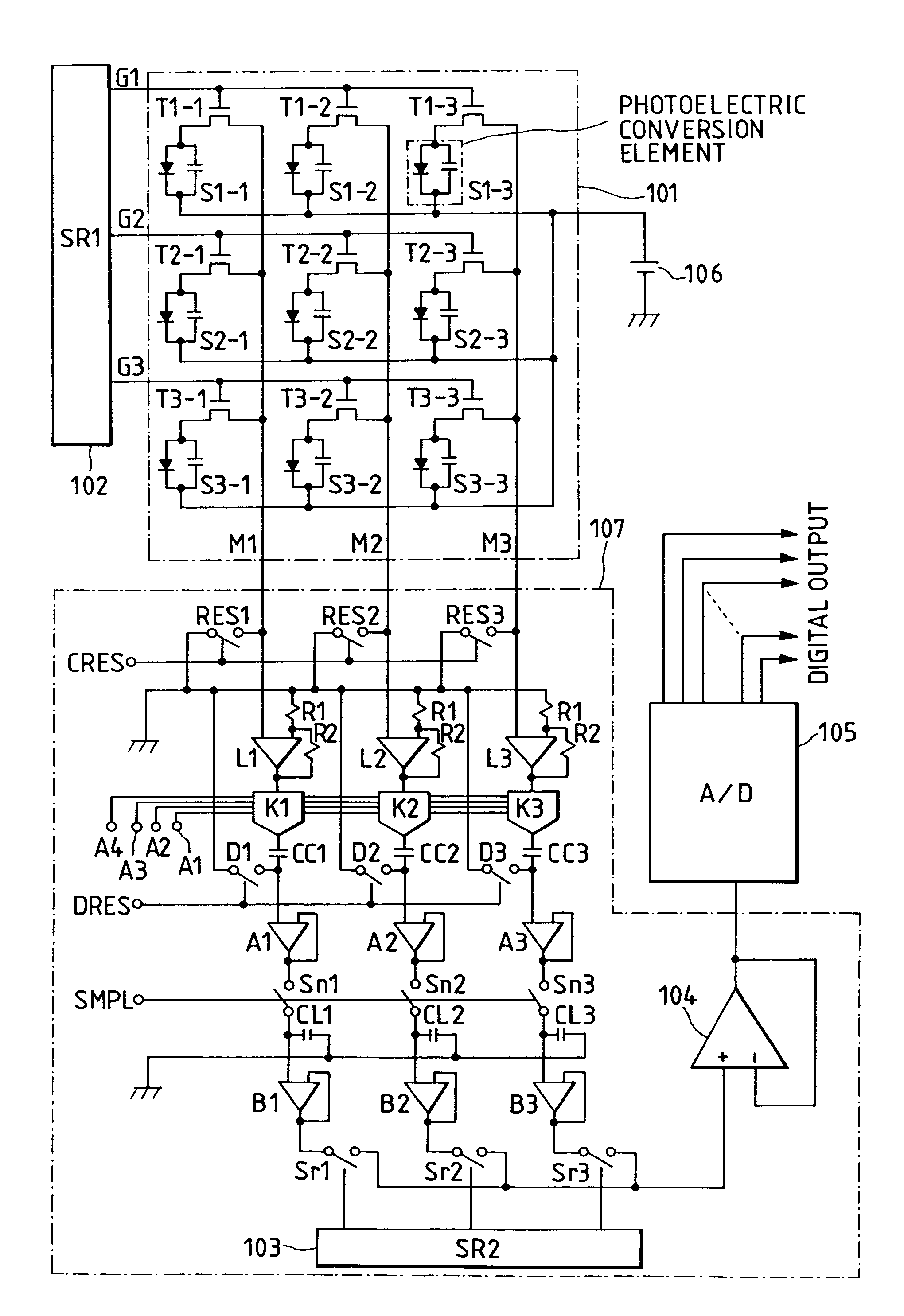
[0111]FIG. 6 is a circuit diagram of a photoelectric conversion apparatus to show the second embodiment of the present invention, which is an example where the photoelectric conversion circuit section is constructed of 3×3=9 pixels. The same constituent members as those in FIG. 3 showing Embodiment 1 are denoted by the same reference symbols and description thereof is omitted herein. FIG. 6 is different from FIG. 3 in that the buffer amplifiers L1 to L3 connected to the respective matrix signal wires in the reading circuit section are replaced by non-inverting amplifiers with an amplification factor G determined by resistors R1, R2. Further, though not shown in FIG. 6, the OP amps of the buffer amplifiers L1 to L3 are excellent in very low noise performance as compared with the other amplifiers. The amplification factor is 1+(R2 / R1).

[0112]In general, the OP amps generate random voltage-nature noise, it is dominated by noise occurring in transistors incorporated, especially in first-...

embodiment 3

[0122]FIG. 8 is a circuit diagram of a photoelectric conversion apparatus to show the third embodiment of the present invention, which is an example in which the photoelectric conversion circuit section is constructed of 3×3=9 pixels. The same constituent members as those in FIG. 6 shown in the second embodiment are denoted by the same reference symbols and description thereof is omitted. FIG. 8 is different from FIG. 6 in that in the reading circuit section capacitor elements CC1 to CC3 for letting only AC components pass are connected to midway of output wires from the output terminals of OP amps L1 to L3 and in that reset switches D1 to D3 for DC restoration of the capacitor elements are provided. Further, a buffer amplifier A1 to A3 for impedance transformation is connected to each capacitor element CC1 to CC3.

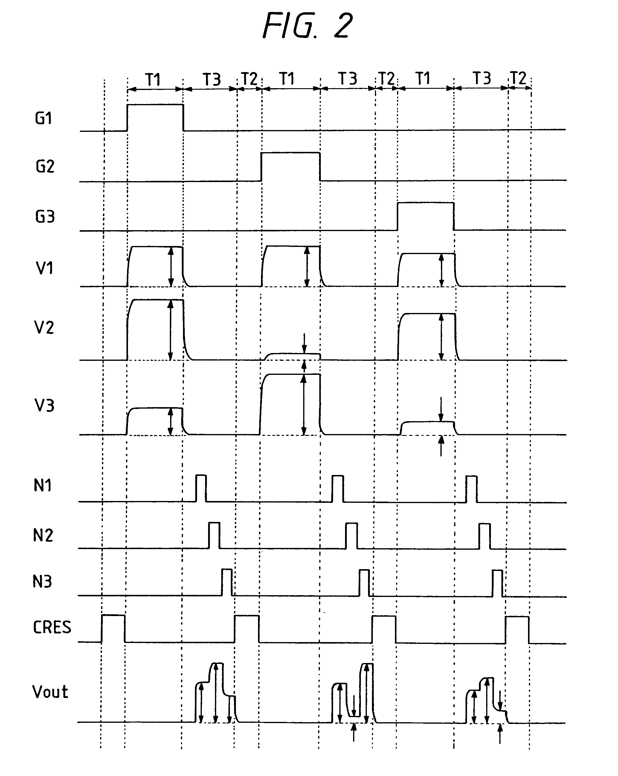
[0123]Also, FIG. 9 is a timing chart to show the operation in FIG. 8, which especially illustrates the operation related to the capacitor elements CC1 to CC3 and reset swi...


PUM


Abstract

In order to provide a photoelectric conversion apparatus, which is an apparatus excellent in reading speed, high S / N, high tone level, and low cost, the photoelectric conversion apparatus has a photoelectric conversion circuit section comprising a plurality of photoelectric conversion elements, switching elements, matrix signal wires, and gate drive wires arranged on a same substrate in order to output parallel signals, a driving circuit section for applying a driving signal to the gate drive wire, and a reading circuit section for converting the parallel signals transferred through the matrix signal wires to serial signals to output them, wherein the reading circuit section comprises at least one analog operational amplifier connected with each of the matrix signal wires, transfer switches for transferring output signals from the respective matrix signal wires, output through each amplifier, reading capacitors, and reading switches for successively reading the signals out of the reading capacitors in the form of serial signals.

Description

[0001]This application is a division of application Ser. No. 08 / 815,532, filed Mar. 12, 1997.BACKGROUND OF THE INVENTION[0002]1. Field of the Invention[0003]The present invention relates to a photoelectric conversion apparatus and a photoelectric conversion system having the apparatus. More particularly, the invention relates to a photoelectric conversion apparatus applicable to X-ray detectors for non-destructive examination such as medical care or internal examination, to image input units for business machines such as digital copiers, electronic blackboards, and facsimile machines, and so on, and also relates to a system having the apparatus.[0004]2. Related Background Art[0005]Presently, the majority of X-ray image pickup apparatus used for medical diagnosis employs a so-called film method in which X-rays are radiated to a human body, then the X-rays transmitted by the human body irradiate a fluorescent member for converting X-rays to visible light, and a film is exposed to fluo...

Claims


Application Information

Patent Timeline
Patent Type & Authority Patents(United States)
IPC IPC(8): H04N3/14H04N1/028H01L31/10H04N1/04H04N5/32H04N5/335H04N5/363H04N5/365H04N5/374H04N5/376H04N5/378
CPCH04N5/32H04N5/335H04N5/363H04N5/365H04N5/3742H04N5/378H01L27/14609H04N25/00H04N25/67H04N25/65H04N25/767H04N25/75
Inventor ENDO, TADAOKAIFU, NORIYUKISATO, TOSHIAKIMORISHITA, MASAKAZU
Owner CANON KK
Why Eureka
Try Eureka