Semiconductor device

a semiconductor and device technology, applied in semiconductor devices, semiconductor/solid-state device details, electrical devices, etc., can solve the problems of corroding electrode posts or connection wirings, disconnection of connection wirings, and difficulty in ensuring sufficient adhesion between the side surface of each post electrode and the sealing resin, so as to prevent the intrusion of moisture, prevent the separation, and prevent the effect of corrosion or disconnection of the connection wiring

Active Publication Date: 2008-11-04
LAPIS SEMICON CO LTD
View PDF9 Cites 7 Cited by
  • Summary
  • Abstract
  • Description
  • Claims
  • Application Information

AI Technical Summary

Benefits of technology

[0008]An object of the present invention is to provide a semiconductor device capable of enhancing the reliability of connection of the semiconductor device and to exclude the influence of ultraviolet rays.
[0010]With such an arrangement, the side surface of the post electrode tightly adheres to the sealing layer via the adhesion film. Therefore, even when an external stress is applied to the post electrode, it becomes possible to prevent the separation between the post electrode and the sealing layer, and to prevent the intrusion of the moisture or the like from outside. Thus, the corrosion or disconnection of the connection wiring can be prevented, and therefore the reliability of connection of the semiconductor device can be enhanced. Moreover, the adhesion film is covered by the sealing layer having light-shielding property, and therefore it becomes possible to prevent the circuit element of the semiconductor device from being exposed to the ultraviolet rays or the like after the semiconductor is mounted on the mounting substrate. Therefore, it becomes possible to prevent the memory of the circuit element from being erased.

Problems solved by technology

However, in the conventional art disclosed in Patent Publication No. 1, since the side surfaces of the post electrodes are sealed by the sealing resin of epoxy resin, it is difficult to ensure sufficient adhesion between the side surface of each post electrode and the sealing resin.
Therefore, when the bump electrodes are bonded to the post electrodes in the mounting process of the semiconductor device on the mounting substrate, a difference in thermal expansion between the semiconductor device and the mounting substrate causes an external force to be concentrated on the post electrodes via the bump electrodes, with the result that the post electrodes and the sealing layer may separate from each other.
In such a case, moisture in the air or the like may intrude through gaps between the post electrodes and the sealing layer, and may cause corrosion of the electrode posts or connection wirings.
If an external force is repeatedly applied to the corroded connection wirings or the like, the disconnection of the connection wirings may occur, or crack may be generated on the lower layer.
Thus, the reliability of connection of the semiconductor device may be degraded.
This problem is noticeable particularly when the post electrodes are formed of copper.

Method used


Image

  • Semiconductor device
  • Semiconductor device
  • Semiconductor device

Examples


first embodiment

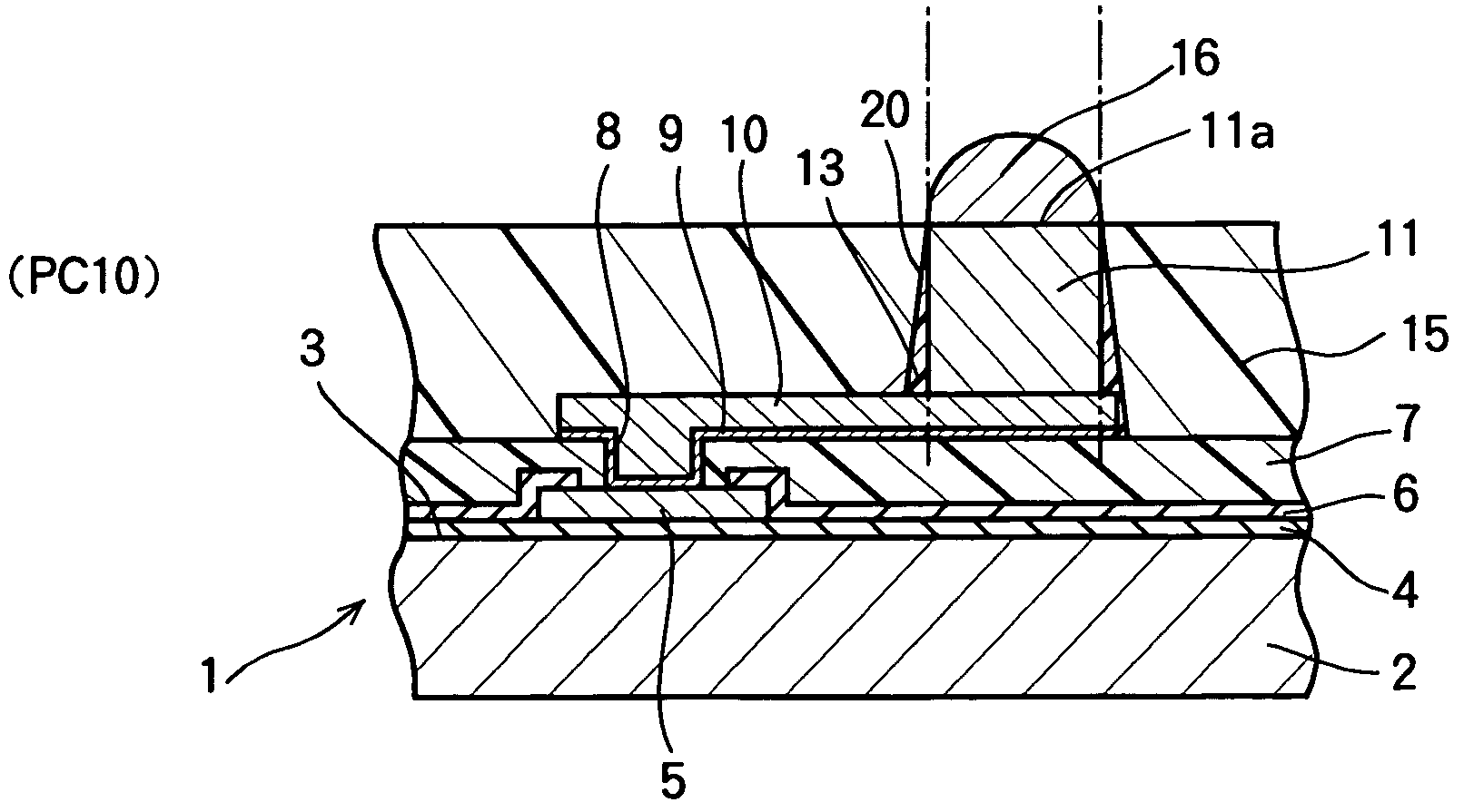
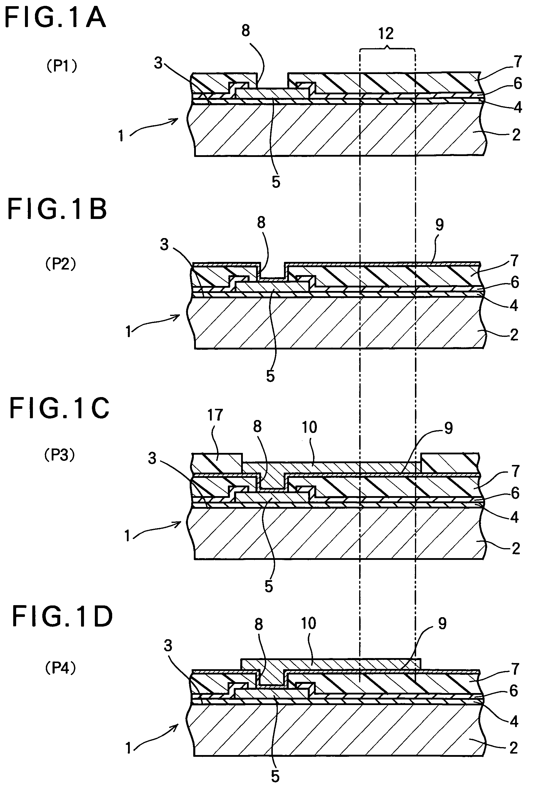
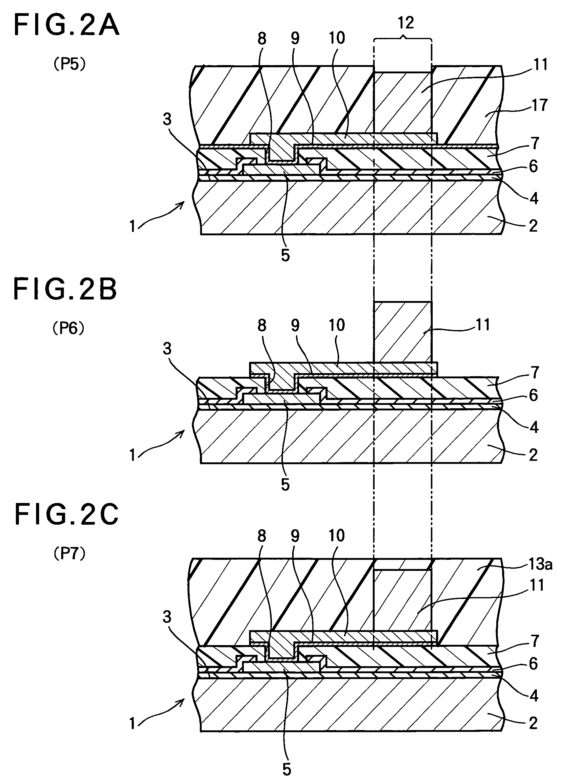
[0026]FIGS. 1A through 1D, FIGS. 2A through 2C and FIGS. 3A through 3C illustrate a manufacturing method of a semiconductor device according to the first embodiment of the present invention. FIGS. 1A through 3C are sectional views of a semiconductor device, and particularly show the vicinity of electrode pads and post electrodes connected to the electrode pads via connection wirings. In FIGS. 1A through 3C, only one electrode pad, one post electrode and one connection wiring are shown.

[0027]As shown in FIGS. 1A through 3C, a numeral 1 denotes a semiconductor wafer for manufacturing a plurality of CSP type semiconductor devices.

[0028]The semiconductor wafer 1 includes a semiconductor substrate 2 composed of silicon. A plurality of circuit elements are formed on the upper surface of the semiconductor substrate 2. The circuit elements are made of semiconductor elements connected to each other via connection wirings. The upper surface of the semiconductor substrate 2 on which the circui...

second embodiment

[0062]FIGS. 4A through 4D, FIGS. 5A through 5C and FIGS. 6A through 6C illustrate a manufacturing method of a semiconductor device according to the second embodiment of the present invention.

[0063]The components of the semiconductor device of the second embodiment that are the same as those of the first embodiment are assigned the same reference numerals, and duplicate explanation will be omitted.

[0064]In the second embodiment, the thickness T (shown in FIG. 6C) of the adhesion film 13 is preferably in the range from 5 μm to 40 μm, as was described in the first embodiment. This is because of the following reason (in addition to the reason described in the first embodiment). If the adhesion film 13 is thinner than 5 μm, there may be cases where the adhesion film 13 is not formed on a stepped portion around the connection wirings 10. In such a case, the difference in thermal expansion between the sealing layer 15 and the connection wirings 10 (during the heat treatment for forming the...

third embodiment

[0079]FIGS. 7A through 7E, FIGS. 8A through 8C, FIGS. 9A through 6C and FIG. 10 illustrate a manufacturing method of a semiconductor device according to the third embodiment of the present invention.

[0080]The components of the semiconductor device of the third embodiment that are the same as those of the first embodiment are assigned the same reference numerals, and duplicate explanation will be omitted.

[0081]In the third embodiment, the thickness T (shown in FIG. 10) of the adhesion film 13 is preferably in the range from 5 μm to 40 μm, as was described in the second embodiment.

[0082]In this embodiment, the thickness of the adhesion film 13 is 10 μm.

[0083]Hereinafter, the manufacturing method of the semiconductor device of the third embodiment will be described with reference to FIGS. 7A through 10.

[0084]The processes PB1 through PB4 shown in FIGS. 7A through 7D are the same as the processes P1 through P4 (FIGS. 1A through 1D) of the first embodiment, and therefore the explanation ...


PUM


Abstract

A semiconductor device includes a semiconductor substrate, an electrode pad electrically connected to a circuit element formed on the semiconductor substrate, a connection wiring electrically connected to the electrode pad and extending on the semiconductor substrate, and a post electrode formed on the connection wiring. The semiconductor device further includes an adhesion film formed on the side surface of the post electrode, and a sealing layer that has light-shielding property and seals the surface of the adhesion film and the connection wiring.

Description

BACKGROUND OF THE INVENTION[0001]This invention relates to a small size semiconductor device as typified by WCSP (Wafer-level Chip Size Package) manufactured by forming a plurality of circuit elements on a semiconductor wafer and dividing the semiconductor wafer into individual pieces. This invention also relates to a manufacturing method of the semiconductor device.[0002]Recently, there is a strong need for reducing the size and thickness of a semiconductor device on which semiconductor elements are mounted. In particular, a CSP (Chip Scale Package) type semiconductor device is mainly used as a thin semiconductor chip. The CSP semiconductor device includes spherical bump electrodes disposed on the upper surface thereof.[0003]A manufacturing method of the conventional CSP type semiconductor device will be described below. Circuit elements are formed on the upper surface of a semiconductor wafer. An insulation layer is formed to cover the circuit elements on the upper surface of the ...

Claims


Application Information

Patent Timeline
Patent Type & Authority Patents(United States)
IPC IPC(8): H01L23/48H01L23/52H01L29/40
CPCH01L23/3114H01L23/552H01L24/13H01L24/11H01L24/02H01L2224/1147H01L2224/13099H01L2924/01013H01L2924/01015H01L2924/01022H01L2924/01029H01L2924/01078H01L2924/01082H01L2924/04941H01L2924/3025H01L2924/01006H01L2924/01033H01L2924/014H01L2224/02166H01L2224/0401H01L2924/00H01L2224/11H01L2224/13H01L24/05H01L2224/05569H01L2224/13024H01L2224/023H01L2924/0001
Inventor WATANABE, KIYONORI
Owner LAPIS SEMICON CO LTD
Why Eureka
Try Eureka