Wafer holder with peripheral lift ring

a technology of lift ring and wafer, which is applied in the direction of coating, metallic material coating process, chemical vapor deposition coating, etc., can solve the problems of increasing the probability of crystallographic slippage, destroying any device through which it may pass, and slipping in the wafer, so as to reduce the effect of thermal shock, and reduce the risk of thermal shock

Inactive Publication Date: 2008-11-11
ASM IP HLDG BV
View PDF47 Cites 19 Cited by
  • Summary
  • Abstract
  • Description
  • Claims
  • Application Information

AI Technical Summary

Benefits of technology

[0014]It is a principle object and advantage of the present invention to provide an improved wafer support system that permits a cold wafer to be loaded into a pre-heated reaction chamber while avoiding the above-mentioned problems associated with thermal shock.
[0015]Prior art susceptors utilizing lift pins can reduce the effects of thermal shock by permitting the loading of a wafer onto the lift pins in their elevated positions. When the wafer is in the elevated position, the wafer temperature can be permitted to increase much more gradually than would occur if the wafer were immediately brought into flush contact with a flat surface of the susceptor. In order to reduce the risk of thermal shock, the wafer can be maintained in the elevated position until the wafer temperature increases to a degree such that the likelihood of thermal shock is substantially reduced or eliminated when the wafer is eventually lowered onto the susceptor surface.
[0016]One problem with lift pins is that they tend to scratch the lower surface of the wafer, which in turn increases the likelihood of crystallographic slip. Slip is a defect in the crystalline structure of the wafer, which destroys any devices through which it may pass. The presence of scratches on a wafer causes slip to occur in the wafer at lower temperatures than if no scratches are present. In other words, the presence of scratches makes a wafer less robust and less able to tolerate high temperatures. Scratches also increase the susceptibility of a wafer to slip under rapidly varying temperature conditions. In addition, scratches cause nodule growth on the backside of the wafer, which leads to alignment problems during photolithography.
[0017]The preferred embodiments of the present invention solve this problem by providing a vertically moveable lift ring that supports the outer radial periphery of a wafer. The lift ring can be raised above the remaining portions of the susceptor to receive a newly loaded wafer. In the raised position, the only heat conduction received by the wafer is via the peripheral lift ring. Heat conduction between the remainder of the susceptor and the raised wafer is substantially prevented. Moreover, heat conduction to the wafer is localized at the wafer periphery, preferably in the exclusion zone of the wafer. When the wafer is in the raised position, the majority of the heat received by the wafer is in the form of (1) radiation from the heated susceptor (from both the lift ring and the remainder of the susceptor), (2) radiation from the heat lamps, if they are on, and (3) convection from warm gas within the chamber. In addition, as indicated above, some heat is received at the wafer edge in the form of conduction from the lift ring. The wafer can be maintained in the raised position until the wafer temperature rises to a level sufficient to substantially prevent or significantly reduce thermal shock to the wafer when the wafer is eventually lowered onto the remainder of the susceptor. The lift ring provides more stable support to the wafer than lift pins. Further, in contrast to lift pins, the lift ring does not have any sharp contact surfaces that might scratch the wafer. The upper surface of the lift ring is preferably flat and only contacts the wafer near its outer radial edge.
[0018]As used herein, heat “conduction” refers to the transfer of energy arising from the temperature difference between adjacent bodies. It is not uncommon for skilled artisans to understand heat conduction to include heat transfer across small gaps. However, for the purposes of the present application, “conduction” does not include heat transfer across small gaps.
[0019]In one aspect, the present invention provides a susceptor for supporting a wafer within a reaction chamber, comprising an inner plug, a lift ring, and a lift device. The inner plug can have a generally flat top surface, a gridded surface including grooves, a concave gridded surface, or other configuration. The lift ring has an upper wafer support surface configured to support a bottom outer peripheral surface of a wafer. The lift ring also has a central aperture positioned such that the lift ring contacts only a peripheral portion of a wafer supported thereon. The central aperture is sized and shaped to closely receive the inner plug. The lift ring has a lowered position in which the wafer support surface is generally at the same vertical position as a top surface of the inner plug. The lift ring also has an elevated position in which the wafer support surface is above the top surface of the inner plug such that a wafer supported on the lift ring substantially does not contact the inner plug. The lift device operates to move the lift ring between its lowered position and its elevated position.

Problems solved by technology

One problem with lift pins is that they tend to scratch the lower surface of the wafer, which in turn increases the likelihood of crystallographic slip.
Slip is a defect in the crystalline structure of the wafer, which destroys any devices through which it may pass.
The presence of scratches on a wafer causes slip to occur in the wafer at lower temperatures than if no scratches are present.
In other words, the presence of scratches makes a wafer less robust and less able to tolerate high temperatures.
In addition, scratches cause nodule growth on the backside of the wafer, which leads to alignment problems during photolithography.

Method used


Image

  • Wafer holder with peripheral lift ring
  • Wafer holder with peripheral lift ring
  • Wafer holder with peripheral lift ring

Examples


Embodiment Construction

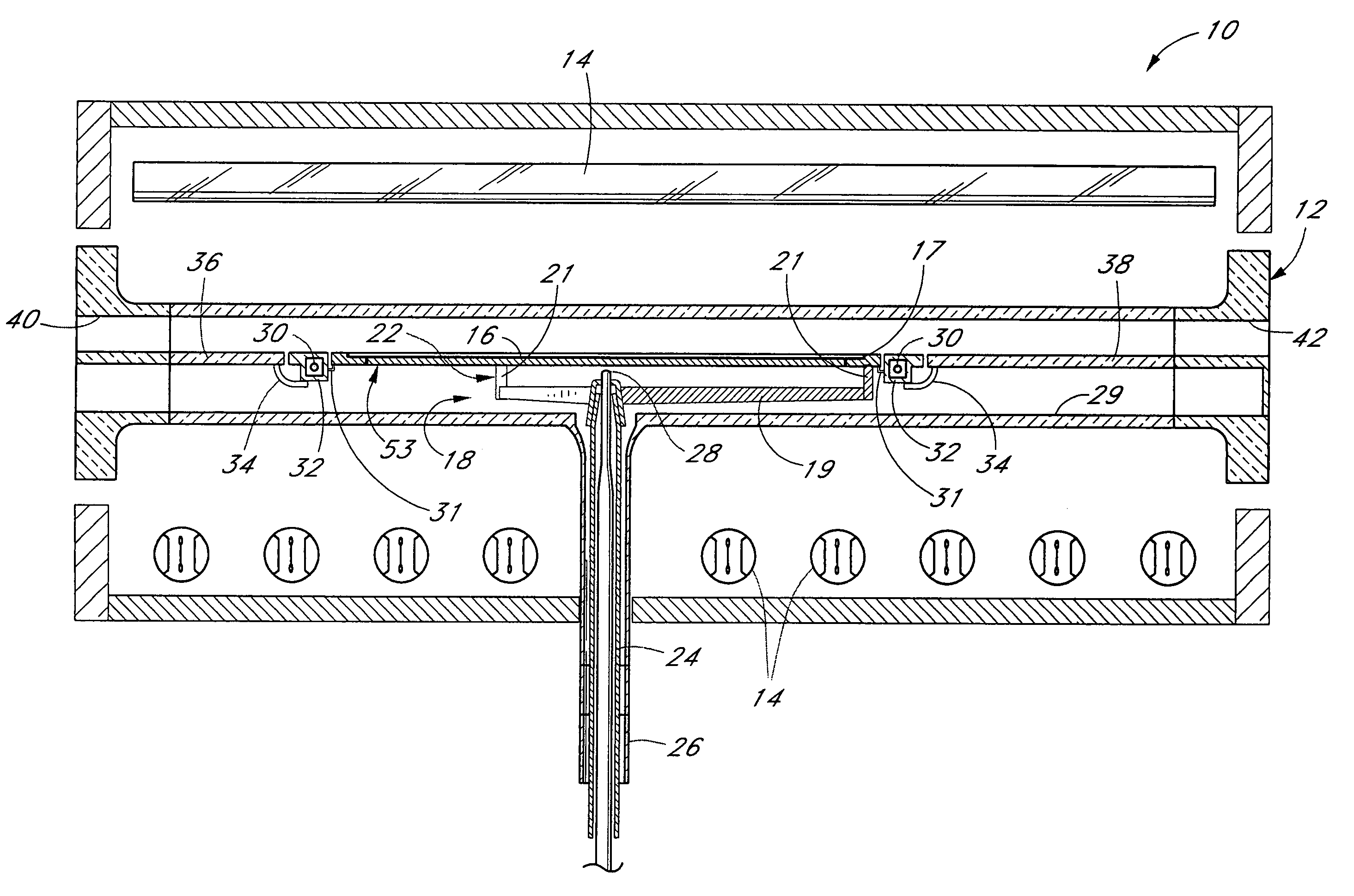
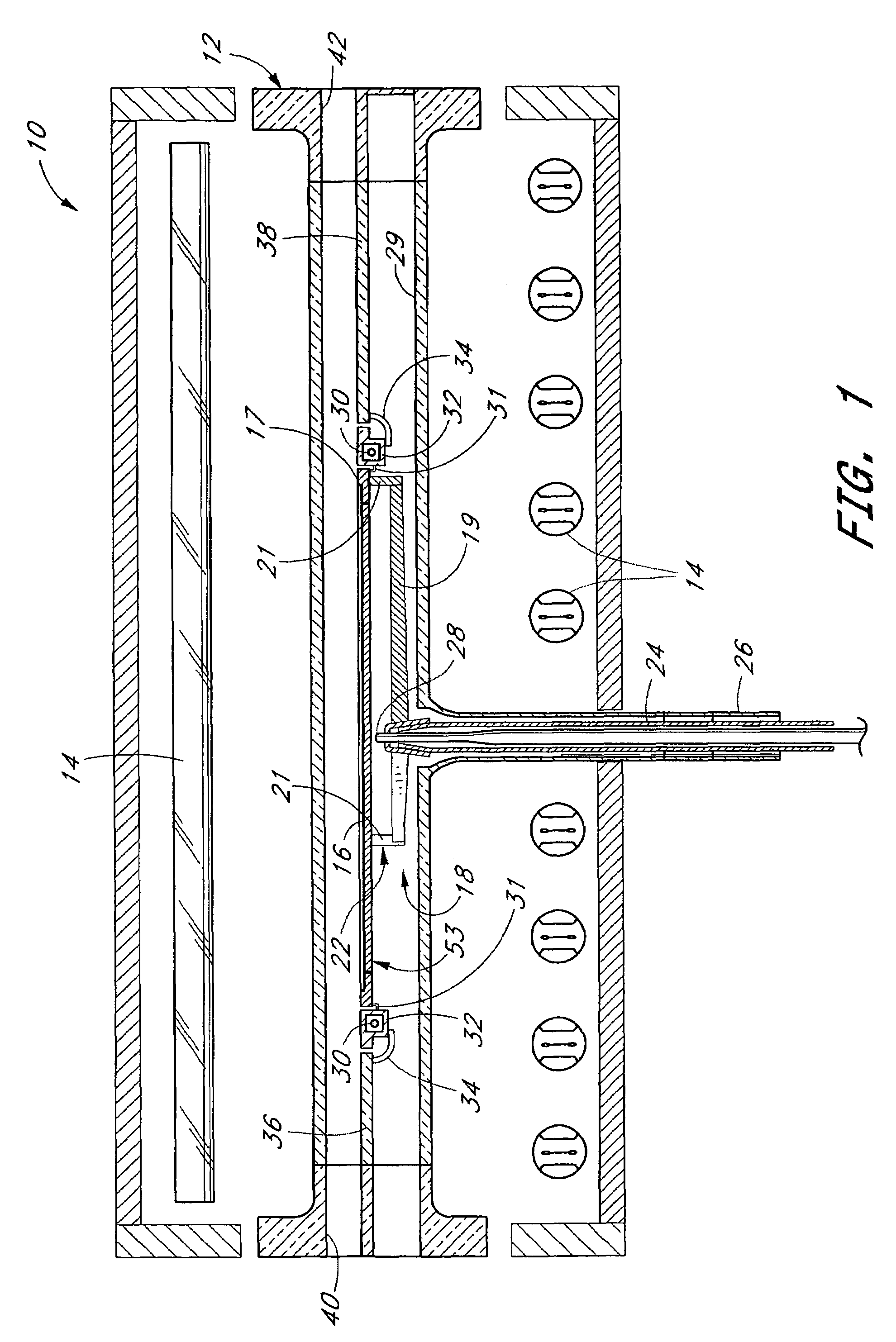
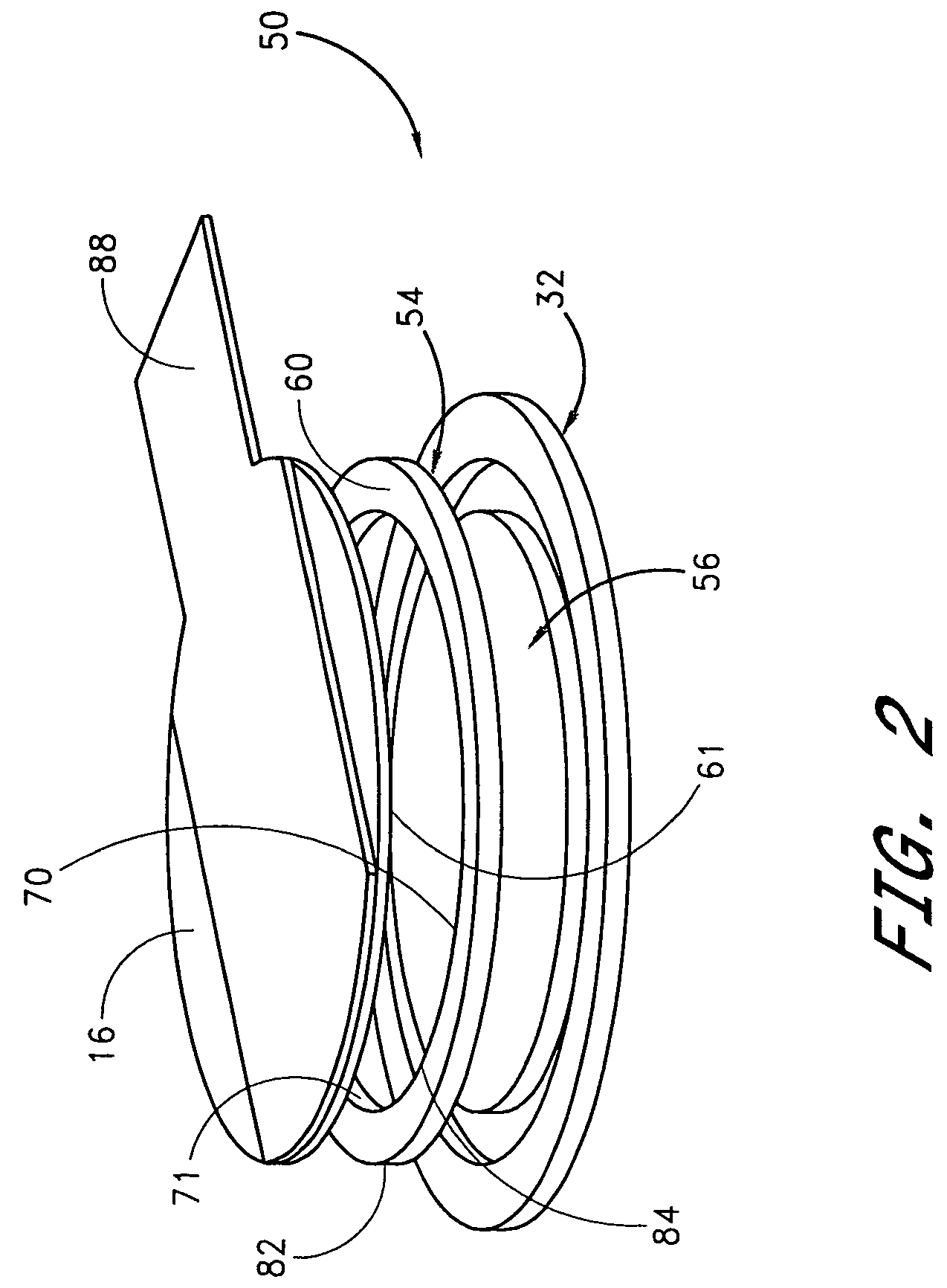
[0048]Contained herein are descriptions of several different embodiments of wafer holders having features in accordance with the teachings of the present invention. It will be understood that these wafer holders can be placed within “hot wall” reactors or “cold wall” reactors. In the latter case, these wafer holders can be susceptors that absorb radiant energy from the heating elements. Various susceptors according to the invention are illustrated and described herein, including susceptor 50 (shown in FIGS. 2-4), susceptor 57 (FIG. 5), susceptor 51 (FIG. 6), and susceptor 53 (FIG. 7), each of which are described in further detail below. Any of these and other susceptors according to the invention can be used within a reactor. FIG. 1 illustrates an exemplary reactor containing the susceptor 53 of FIG. 7. The skilled artisan will understand that any of the herein illustrated susceptors can be provided within the reactor illustrated in FIG. 1.

[0049]As explained above, FIG. 1 illustrate...


PUM

PropertyMeasurementUnit
temperaturesaaaaaaaaaa
anglesaaaaaaaaaa
temperatureaaaaaaaaaa

Abstract

A wafer holder for supporting a wafer within a CVD processing chamber includes a vertically moveable lift ring configured to support the bottom peripheral surface of the wafer, and an inner plug having a top flat surface configured to support the wafer during wafer processing. The lift ring has a central aperture configured to closely surround the inner plug. When a wafer is to be loaded onto the wafer holder, the lift ring is elevated above the inner plug. The wafer is loaded onto the lift ring in the elevated position. Then, the lift ring is maintained in the elevated position for a time period sufficient to allow the wafer temperature to rise to a level that is sufficient to significantly reduce or even substantially prevent thermal shock to the wafer when the wafer is brought into contact with the inner plug. The lift ring is then lowered into surrounding engagement with the inner plug. This is the wafer processing position of the wafer holder.

Description

REFERENCE TO RELATED APPLICATIONS[0001]The present application is a divisional of U.S. patent application Ser. No. 10 / 100,308, filed Mar. 15, 2002 now U.S. Pat. No. 6,776,849.BACKGROUND OF THE INVENTION[0002]1. Field of the Invention[0003]This invention relates generally to supports for wafers in semiconductor processing chambers and, more particularly, to a wafer holder for supporting a wafer within a cold wall chemical vapor deposition chamber.[0004]2. Description of the Related Art[0005]High-temperature ovens, or reactors, are used to process semiconductor wafers from which integrated circuits are made for the electronics industry. A substrate, typically a circular silicon wafer, is placed on a wafer holder. If the wafer holder helps to attract heat, it is called a susceptor. The wafer and wafer holder are enclosed in a quartz chamber and heated to high temperatures, such as 600° C. (1112° F.) or higher, by a plurality of radiant lamps placed around the quartz chamber. A reactant...

Claims


Application Information

Patent Timeline
Patent Type & Authority Patents(United States)
IPC IPC(8): C23C16/00C23F1/00H01L21/306C23C16/458C23C16/48H01L21/687
CPCC23C16/4584C23C16/4585C23C16/481H01L21/68735H01L21/68742
Inventor AGGARWAL, RAVINDER K.KEETON, TONY J.GOODMAN, MATTHEW G.
Owner ASM IP HLDG BV
Why Eureka
Try Eureka