Method for manufacturing and structure for transistors with reduced gate to contact spacing

Inactive Publication Date: 2008-12-02
TEXAS INSTR INC
View PDF7 Cites 0 Cited by
  • Summary
  • Abstract
  • Description
  • Claims
  • Application Information

AI Technical Summary

Benefits of technology

[0006]The present invention provides a method that substantially reduces or eliminates at least some of the disadvantages and problems associated with previously developed methods for manufacturing transistors. Accordingly, in certain embodiments, the present invention provides a method that allows an inhibitin

Problems solved by technology

The demand for microprocessors to be made smaller is ever present because size reduction typically increases speed and decreases power consumption.
These inhibiting materials may often be applied to only inhibit the effects of a particular manufacturing step and, thus, may be of limited usefulness after they have served this purpose.
Unfortunately, once these limited purpose inhibiting materials have served their purpose, they may be difficult to remove.
For example, s

Method used


Image

  • Method for manufacturing and structure for transistors with reduced gate to contact spacing
  • Method for manufacturing and structure for transistors with reduced gate to contact spacing
  • Method for manufacturing and structure for transistors with reduced gate to contact spacing

Examples


Example

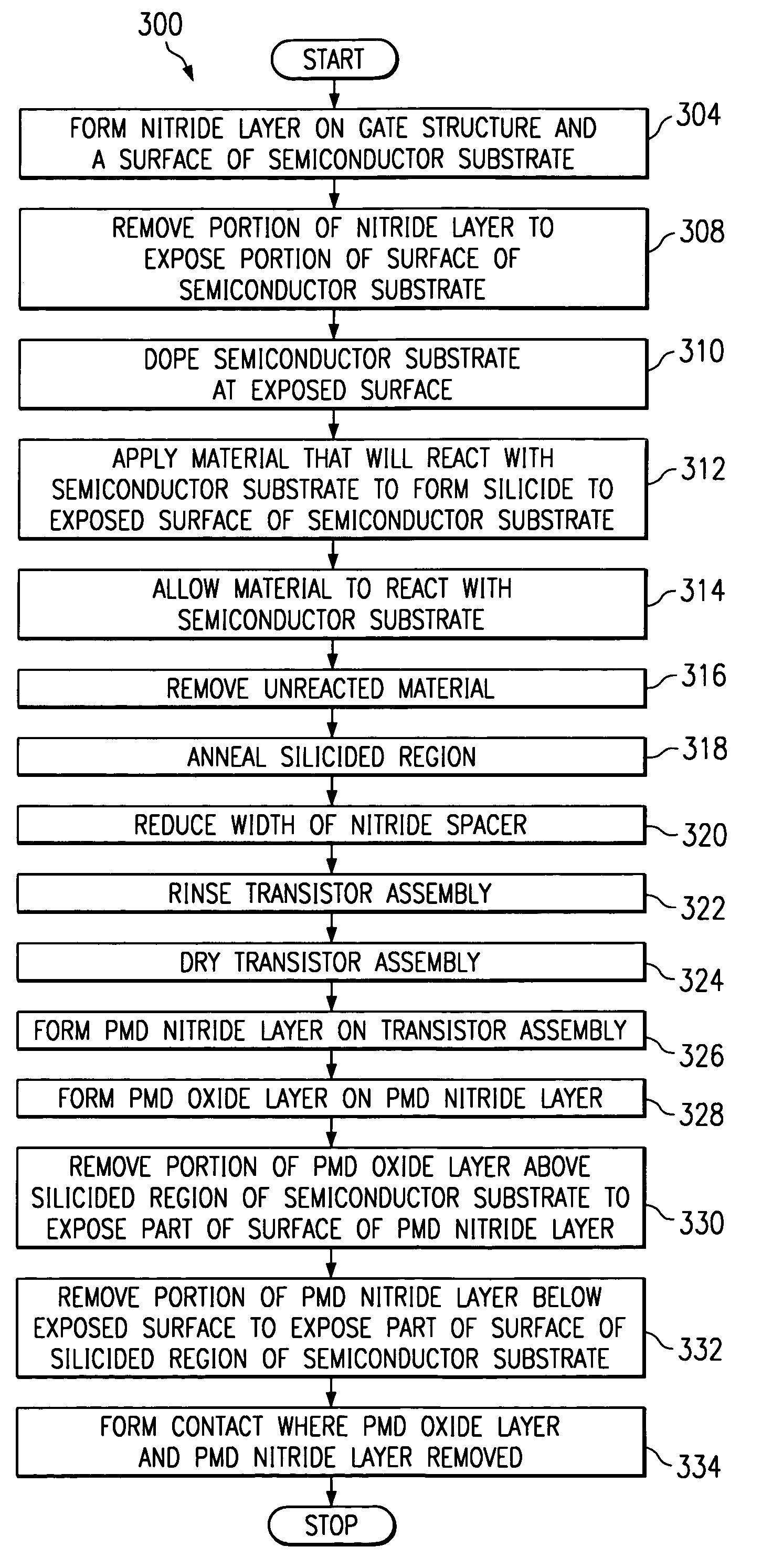
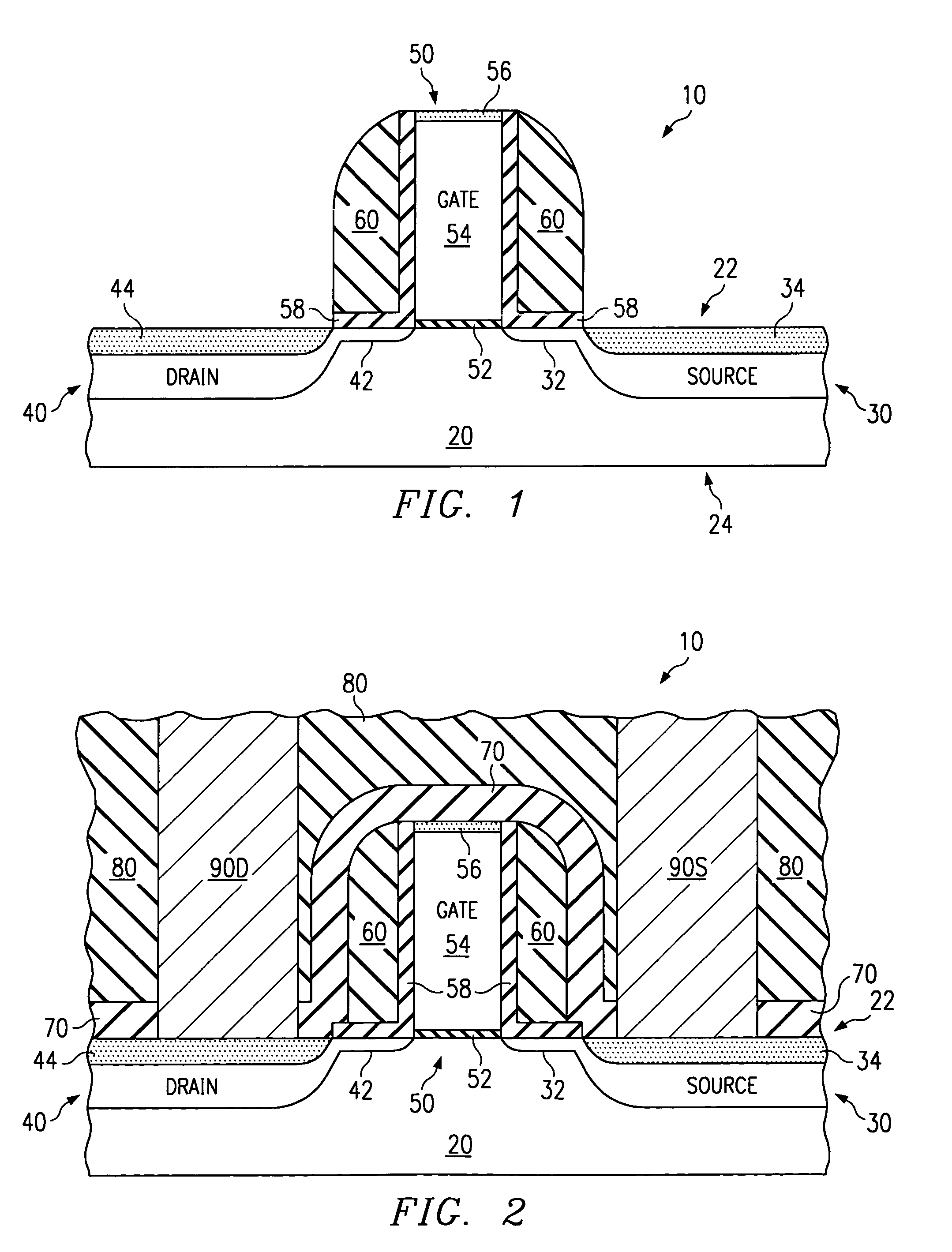
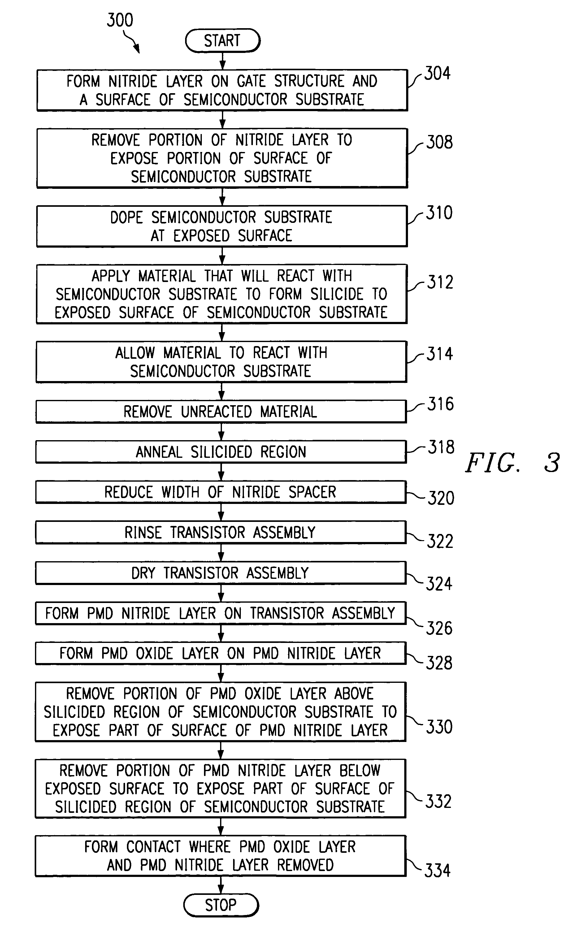
[0015]FIG. 1 illustrates a transistor assembly 10 at one stage of a manufacturing process in accordance with the present invention. In general, transistor assembly 10 includes a semiconductor layer 20, a source region 30 formed in semiconductor layer 20, a drain region 40 formed in semiconductor layer 20, a gate structure 50, and a spacer layer 60.

[0016]Semiconductor layer 20 may be a substrate, such as, for example, a wafer, and may be composed of any appropriate type of semiconductive material. In the illustrated embodiment, semiconductor layer 20 is composed of single crystalline silicon and has a first surface 22 and a second surface 24. Semiconductor layer 20 may also be a layer of semiconductive material formed on a substrate. For example, semiconductor layer 20 may be an epitaxial layer grown on a wafer. Semiconductor layer 20 forms a base for the other components of transistor assembly 10 and also serves as a semiconductive material.

[0017]Semiconductor layer 20 includes a so...


PUM


Abstract

A method for manufacturing a transistor includes providing a transistor assembly having a semiconductor layer with a first surface, a dielectric layer disposed on the first surface, a gate electrode disposed on the dielectric layer, an insulation layer adjacent at least part of the gate electrode, and a nitride spacer layer adjacent at least part of the insulation layer. The method also includes depositing, on part of the first surface, a material that will react with the semiconductor layer to form silicide and removing the unreacted material. The method further includes etching the nitride spacer layer, depositing a pre-metal spacer layer adjacent at least part of the nitride spacer layer and at least part of the first surface, etch removing a portion of the pre-metal spacer layer to expose part of the silicided portion of the first surface, and forming a contact with the silicided portion of the first surface.

Description

[0001]This application is a divisional of application Ser. No. 10 / 068,014, filed Feb. 5, 2002 now U.S. Pat. No. 6,767,777.TECHNICAL FIELD OF THE INVENTION[0002]This invention relates generally to transistors and, more specifically, to a method for manufacturing transistors.BACKGROUND OF THE INVENTION[0003]The demand for microprocessors to be made smaller is ever present because size reduction typically increases speed and decreases power consumption. Generally, making microprocessors smaller entails making the components of the microprocessors smaller. Transistors are one of the basic components of microprocessors. Thus, reducing the size of transistors enables microprocessors to be made smaller and, hence, have increased performance.[0004]Transistors are typically manufactured by forming layers of material on top of one another with some type of processing being performed on each layer before depositing the next layer. Because some of the steps in the processing affect the entire d...

Claims


Application Information

Patent Timeline
IPC IPC(8): H01L31/062H01L31/113H01L21/336H01L21/60H01L29/78
CPCH01L21/76897H01L29/6656H01L29/6659H01L29/7833
Inventor JOYNER, KEITH A.RODDER, MARK S.
Owner TEXAS INSTR INC
Why Eureka
Try Eureka