Stacked three dimensional photonic crystal, light emitting device, and image display apparatus

a three-dimensional photonic crystal and light emitting device technology, applied in the direction of active medium materials, instruments, semiconductor lasers, etc., can solve the problems of high light emitting efficiency, insufficient reflection multi-layer film reflectance, and high probability of heating value increas

Inactive Publication Date: 2008-12-09
CANON KK
View PDF4 Cites 44 Cited by
  • Summary
  • Abstract
  • Description
  • Claims
  • Application Information

AI Technical Summary

Problems solved by technology

In this case, reflectance of a reflection multi-layer film is insufficient to light having a specific wavelength.
Therefore, in each unit light-emitting device, high light emitting efficiency is not obtained and a heating value is likely to increase.
As a result, for example, when a plurality of light emitting devices, each of which can emit light having a plurality of wavelength regions are integrated to form a display apparatus, it is hard to sufficiently improve an integration density because of an increase in heating value.
Therefore, it is hard to perform mode pattern control of light confined in a resonator in-plane direction.
In contrast to this, when the photonic crystal is used for the light emitting structure, it is hard to control a wavelength region of a complete photonic band gap which can be realized by the three-dimensional photonic crystal.
Therefore, it is hard to control all light corresponding to the wavelengths of R, G, and B using the single three-dimensional photonic crystal.
However, a material that is transparent in a visible wavelength region generally has a low refraction index, so that it is hard to obtain a wide PBG (material: refraction index, TiO2: 2.3, Ta2O5: 2.1, CeO2: 2.05, ZrO2: 2.03, GaN: 2.4, LiNbO3: 2.2, LiTaO3: 2.1, and BaTiO3: 2.3).
Therefore, it is hard to realize wide band operation in the case where a use wavelength region is particularly the visible wavelength region.

Method used


Image

  • Stacked three dimensional photonic crystal, light emitting device, and image display apparatus
  • Stacked three dimensional photonic crystal, light emitting device, and image display apparatus
  • Stacked three dimensional photonic crystal, light emitting device, and image display apparatus

Examples


embodiment 1

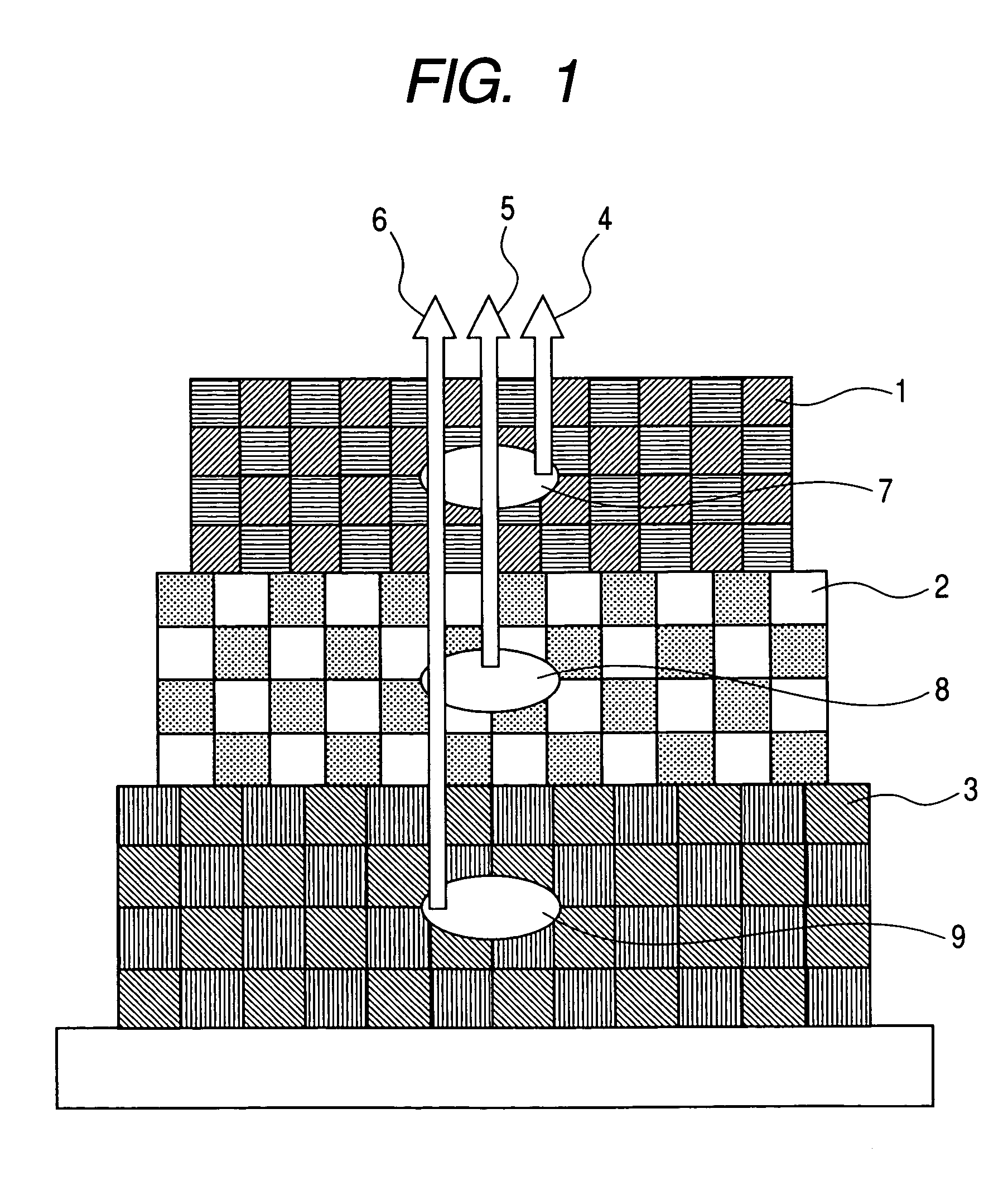
[0073]FIG. 12 is a schematic view showing a stacked light-emitting structure of a current injection excitation type. Three photonic crystal layers that resonate light beams 1201a to 1201c having wavelengths different from one another and emit the light beams are stacked. Each of the photonic crystals has a light-emitting region that includes a point defect resonator and a light emitting medium. Tables 5 and 6 show photonic crystal structures 1204ato 1204c and point defect resonators 1205a to 1205c.

[0074]

TABLE 5FirstSecondThirdphotonicphotonicphotoniccrystalcrystalcrystalstructurestructurestructureGratingInverseInverseInversestructurediamonddiamond opaldiamond opalopalstructurestructurestructureConstituentTiO2TiO2 (n = 2.33)TiO2Material 4(n = 2.33)(n = 2.33)(refractionindex)ConstituentAir orAir or vacuumAir orMaterial 5vacuum(n = 1.00)vacuum(refraction(n = 1.00)(n = 1.00)index)Latticea = 300 nma = 365 nma = 432 nmperiodRadius of0.30a0.30a0.30aconstituentMaterial 5Band gap428 nm to521...

embodiment 2

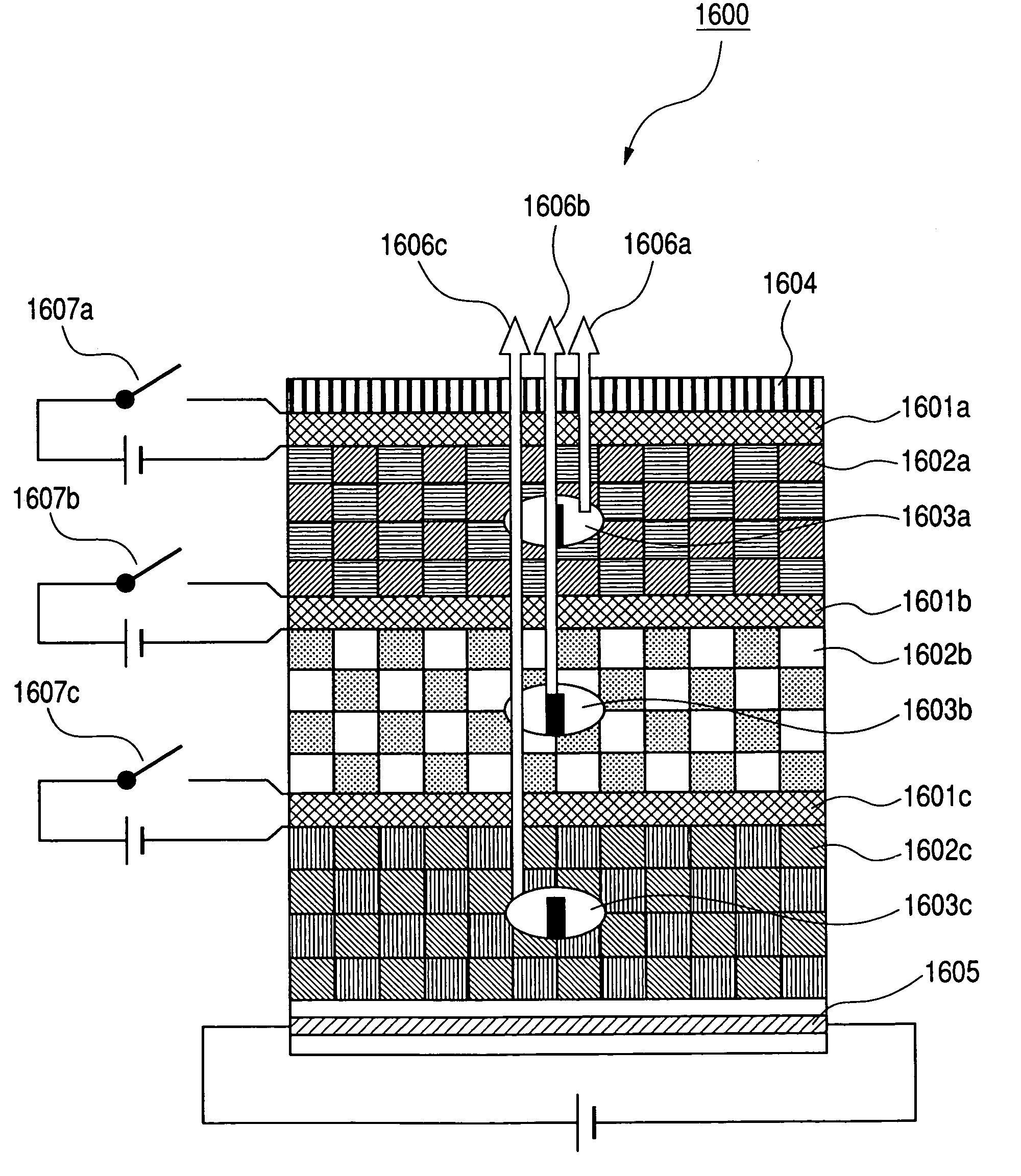
[0097]FIG. 16 shows a stacked light-emitting structure 1600 of an ultraviolet light excitation type. Three photonic crystal layers are stacked. A first photonic crystal layer is composed of a photonic crystal 1602a, a point defect resonator 1603a, and a switching layer 1601a. A second photonic crystal layer is composed of a photonic crystal 1602b, a point defect resonator 1603b, and a switching layer 1601b. A third photonic crystal layer is composed of a photonic crystal 1602c, a point defect resonator 1603c, and a switching layer 1601c. An ultraviolet light source 1605 that emits light having a wavelength capable of exciting fluorescent materials provided in the point defect resonators 1603a to 1603c is located in the lowest layer of the structure 1600. A wavelength selective filter 1604 that cuts off only light emitted from the ultraviolet light source 1605 is provided in the uppermost layer of the structure 1600.

[0098]The fluorescent materials provided in the point defect resonat...

embodiment 3

[0106]Next, a deviation in light extraction efficiency due to a change in stack order of photonic crystal layers will be described. FIG. 17 is a schematic view showing a stacked three-dimensional photonic crystal. Three-dimensional photonic crystal layers 1701b, 1701g, and 1701r including point defect resonators 1702b, 1702g, and 1702r are stacked on a substrate 1700. Table 7 shows the three three-dimensional photonic crystal structures (1701b, 1701g, and 1701r).

[0107]

TABLE 7Structure1701b1701g1701rGratingInverseInverseInversestructurediamonddiamonddiamondopalopalopalConstituentTiO2TiO2TiO2Material 6(n = 2.33)(n = 2.33)(n = 2.33)(refractionindex)ConstituentAir (orAir (orAir (orMaterial 7vacuum)vacuum)vacuum)(refraction(n = 1.00)(n = 1.00)(n = 1.00)index)Dispersion layer0.30a0.30a0.30aradius(a means(a means(a meanslatticelatticelatticeperiod.)period.)period.)Lattice period300 nm365 nm432 nm(a)Resonant450 nm530 nm640 nmwavelength

[0108]The case where the three three-dimensional photoni...


PUM

PropertyMeasurementUnit
wavelength bandaaaaaaaaaa
dielectric constantaaaaaaaaaa
transmittanceaaaaaaaaaa

Abstract

Provided is a light emitting structure which can emit light having a plurality of wavelength distributions from a single light emitting structure, can be integrated at high density, and can control a radiation mode pattern of radiation light and polarization thereof. A stacked three-dimensional photonic crystal is composed of a plurality of three-dimensional photonic crystals having photonic band gaps different from one another, which are stacked. Each of the plurality of three-dimensional photonic crystals includes a resonator in which a point defect is formed.

Description

BACKGROUND OF THE INVENTION[0001]1. Field of the Invention[0002]The present invention relates to a structure capable of selectively emitting multiple-wavelength light using a photonic crystal.[0003]2. Related Background Art[0004]Up to now, several methods of selectively emitting light having a predetermined wavelength have been known. Such a method is broadly classified into an active light emitting method and a passive light emitting method. With respect to the active light emitting method, there are, for example, a method using a light emitting diode and a method using plasma light emission. Light is emitted with a specific wavelength determined according to a medium to be used. A method of applying excitation energy to a fluorescent material to obtain light having a desirable wavelength has been also known. A method using a wavelength selective filter capable of transmitting only light having a specific wavelength, of light having a relatively wide wavelength region, such as whit...

Claims


Application Information

Patent Timeline
Patent Type & Authority Patents(United States)
IPC IPC(8): H01L33/00H01S3/082G02F1/13H01S3/081H01S3/0915H01S3/16H01S3/23H01S5/10H01S5/183H01S5/30H01S5/327H01S5/36H01S5/40H01S5/42H04N9/30H04N9/31
CPCH01S5/426H04N9/30H04N9/3129H01S5/105H01S5/18397H01S5/3086H01S5/327H01S5/36H01S5/4093H01S5/11
Inventor HOSHI, HIKARUTAKAGI, AKINARI
Owner CANON KK
Why Eureka
Try Eureka