Integrated circuit design closure method for selective voltage binning

a technology of integrated circuit design and selective voltage, which is applied in the direction of cad circuit design, program control, instruments, etc., can solve the problems of static power consumption, insignificant portion of overall power consumption, and large amount of power required to opera

Inactive Publication Date: 2009-01-06
GLOBALFOUNDRIES INC
View PDF15 Cites 53 Cited by
  • Summary
  • Abstract
  • Description
  • Claims
  • Application Information

AI Technical Summary

Problems solved by technology

Dynamic power consumption refers to the amount of power required to operate (i.e., switch) a device.
In the past static power consumption was an insignificant portion of overall power consumption.
However, with device scaling the ratio of static to dynamic power making up overall power consumption has increased.
In addressing the issue of static power consumption, designers have realized that manufacturing variations are a critical problem.
Chips that are fabricated either at the “slow” end or the “fast” end of a process distribution (e.g., a process-temperature-variation (PVT) space) may not be desirable.
For example, chips that are fabricated at the “slow” end of such a process distribution may not meet the desired performance specification (i.e., may not have a fast enough switching speed), whereas chips fabricated at the “fast” end of this process distribution may exhibit excessive power and leakage current.
However, as process control has become more and more difficult, timing closure over the full process distribution has become quite challenging.

Method used


Image

  • Integrated circuit design closure method for selective voltage binning
  • Integrated circuit design closure method for selective voltage binning
  • Integrated circuit design closure method for selective voltage binning

Examples


Embodiment Construction

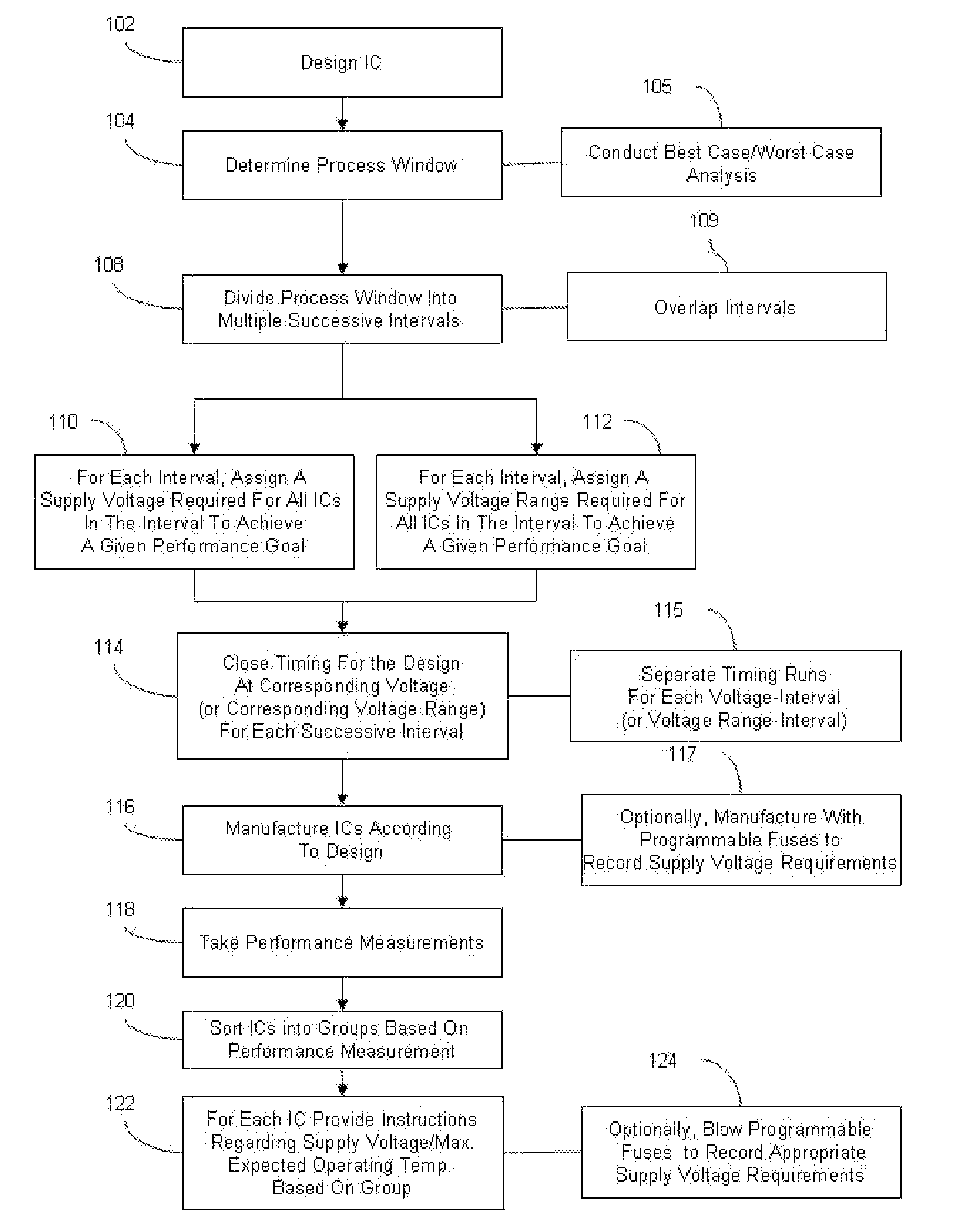
[0026]The embodiments of the invention and the various features and advantageous details thereof are explained more fully with reference to the non-limiting embodiments that are illustrated in the accompanying drawings and detailed in the following description. It should be noted that the features illustrated in the drawings are not necessarily drawn to scale. Descriptions of well-known components and processing techniques are omitted so as to not unnecessarily obscure the embodiments of the invention. The examples used herein are intended merely to facilitate an understanding of ways in which the embodiments of the invention may be practiced and to further enable those of skill in the art to practice the embodiments of the invention. Accordingly, the examples should not be construed as limiting the scope of the embodiments of the invention.

[0027]As mentioned above, it would be advantageous over the prior art to provide a method of designing and manufacturing a chip that combines th...


PUM


Abstract

Disclosed are embodiments of a method of designing and producing an integrated circuit. During the pre-release chip design process, the method subdivides the overall process window for an integrated circuit design into smaller successive intervals corresponding to achievable performance. Each performance interval is independently optimized for performance versus power by assigning to each interval a different corresponding supply voltage. Timing for the design is then closed for each interval at each assigned voltage. After chip manufacturing, the method measures the performance of the integrated circuits that are manufactured according to the design. Using these performance measurements, the circuits are sorted into bins corresponding to each performance interval and appropriately labeled (e.g., with the performance goal and previously assigned supply voltage corresponding to the performance interval).

Description

BACKGROUND[0001]1. Field of the Invention[0002]The embodiments of the invention generally relate to selective voltage binning and, more particularly, an integrated circuit design timing closure method for selective voltage binning.[0003]2. Description of the Related Art[0004]Consumers continue to demand smaller electronic devices with ever small power requirements. Power consumption from the complementary metal oxide semiconductor (CMOS) integrated circuits commonly used to build such electronic devices consists of two components: dynamic (active) power consumption and static (leakage) power consumption. Dynamic power consumption refers to the amount of power required to operate (i.e., switch) a device. Dynamic power consumption is a function of capacitance, voltage, and switching frequency. That is P=CV2F, where P is the dynamic power, C is the effective switch capacitance, V is the supply voltage and F is the switching frequency. Static power consumption refers to the amount of po...

Claims


Application Information

Patent Timeline
Patent Type & Authority Patents(United States)
IPC IPC(8): G06F17/50
CPCG06F17/5045G06F30/30
Inventor KUEMERLE, MARK W.LICHTENSTEIGER, SUSAN K.STOUT, DOUGLAS W.WEMPLE, IVAN L.
Owner GLOBALFOUNDRIES INC
Why Eureka
Try Eureka