Flip-chip packaging process using copper pillar as bump structure

a technology of copper pillars and flip-chips, which is applied in the direction of sustainable manufacturing/processing, final product manufacturing, and semiconductor/solid-state device details. it can solve the problems of difficult control of the step of etching the ubm layer, insufficient strength and capacitance density of the solder bumps b>60/b>, and difficult control of the etching selectivity

Active Publication Date: 2009-01-13
ADVANCED SEMICON ENG INC
View PDF7 Cites 52 Cited by
  • Summary
  • Abstract
  • Description
  • Claims
  • Application Information

AI Technical Summary

Benefits of technology

[0009]Therefore, an aspect of the present invention is to provide a flip-chip packaging process for replacing solder bumps with copper pillars, thereby overcoming the shortcomings of insufficient strength and capacitance density of the solder bumps and requiring relfow steps, thus meanwhile benefiting the controllability of the step for etching the UBM layer.
[0012]Hence, with the application of the present invention, a copper pillar having the features of high strength and high capacitance density is used as a bump structure for meeting the requirements of fabricating high-speed charging and discharging elements, and benefiting the controllability of the step for etching the UBM layer; no reflow steps are required, thus simplifying the processing steps; and the solder covers substantially all of the external surfaces of the copper pillar, thereby preventing the copper pillar from oxidation.

Problems solved by technology

However, since the etching selectivity between the solder bumps 60 and the UBM layer 22 is poor, the step of etching the UBM layer 22 is difficult to be controlled.
Further, the strength and capacitance density of the solder bumps 60 are not sufficient for fabricating high-speed charging and discharging elements.
In addition, the conventional process needs to use the reflow steps, thus making the entire process quite complicated.
Hence, there is a need to develop a flip-chip packaging process using a copper pillar as a bump structure for overcoming the conventional process's disadvantages of insufficient strength and capacitance density of the solder bumps; having difficulty in controlling the step for etching the UBM layer; and requiring the relfow steps.

Method used


Image

  • Flip-chip packaging process using copper pillar as bump structure
  • Flip-chip packaging process using copper pillar as bump structure
  • Flip-chip packaging process using copper pillar as bump structure

Examples


Embodiment Construction

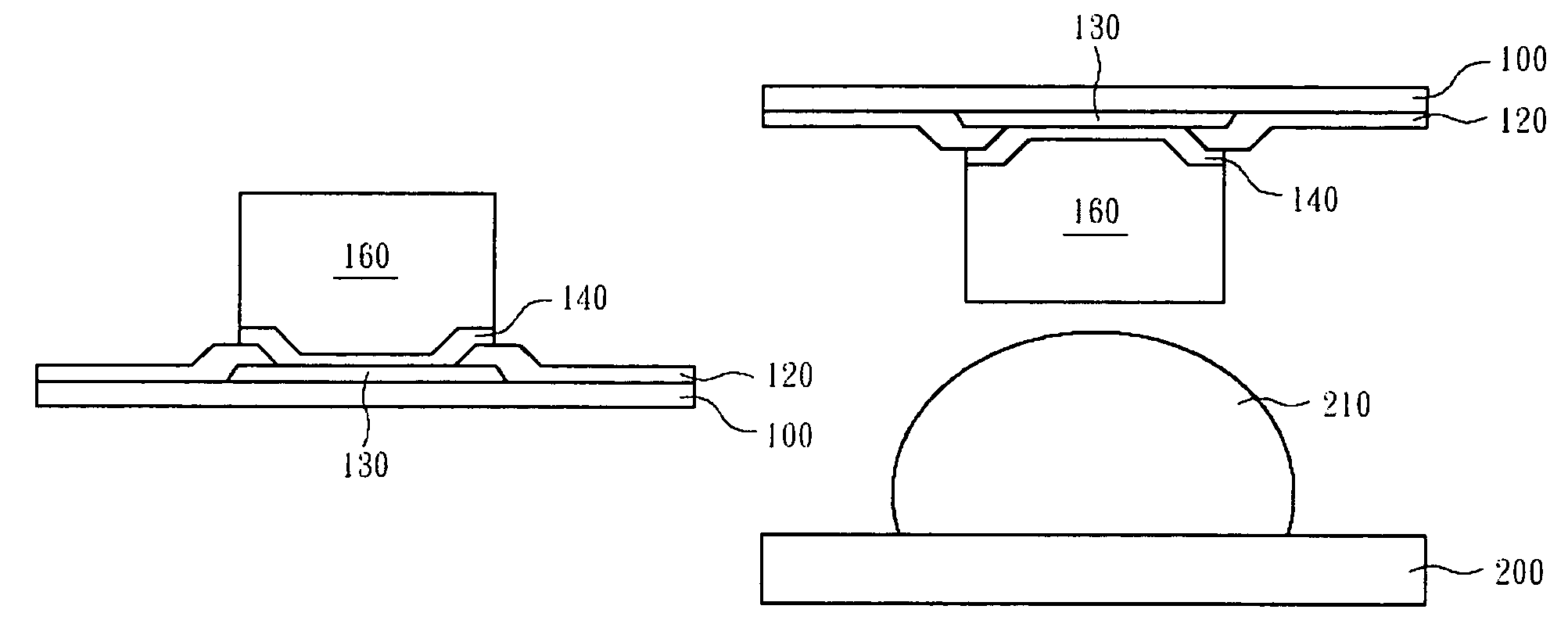
[0019]The present invention is featured in forming a copper pillar on a wafer; forming a solder on a substrate; and covering substantially all of the external surfaces of the pillar with the solder.

[0020]Referring to FIG. 2A to FIG. 2C, FIG. 2A to FIG. 2C are schematic diagrams showing the structure of a copper pillar and the fabrication process thereof in accordance with a preferred embodiment of the present invention. Such as shown in FIG. 2A, a bond pad 130 and a passivation layer 120 are first formed sequentially on a wafer 100, wherein the passivation layer 120 exposes a portion of the bond pad 130. Then, an UBM layer 140 is formed over the bond pad 130 and the passivation layer 120. Thereafter, a photoresist layer 150 is formed on the UBM layer 140 with an opening (not labeled) formed for exposing a portion of the UBM layer 140. Then, such as shown in FIG. 2B, a copper material 160 is filled into the opening. Thereafter, such as shown in FIG. 2C, the photoresist layer 150 and ...


PUM

PropertyMeasurementUnit
distanceaaaaaaaaaa
temperatureaaaaaaaaaa
distanceaaaaaaaaaa

Abstract

A flip-chip packaging process is disclosed. The present invention is featured in forming a copper pillar on a wafer, forming a solder on a substrate; and enabling the solder to substantially cover the entire externally-exposed surface of the copper pillar, thereby connecting the copper pillar to the substrate. The copper pillar of the present invention can be such as a prism or a cylinder.

Description

RELATED APPLICATIONS[0001]The present application is based on, and claims priority from, Taiwan Application Serial Number 94130921, filed Sep. 8, 2005, the disclosure of which is hereby incorporated by reference herein in its entirety.FIELD OF THE INVENTION[0002]The present invention relates to a flip-chip packaging process, and more particularly to the flip-chip packaging process using a copper pillar as a bump structure.BACKGROUND OF THE INVENTION[0003]Whenever an integrated circuit (IC) is fabricated, it still needs to be connected to other elements; implemented with heat dissipation function; and protected by a housing, and thus a semiconductor packaging process follows. Semiconductor package structures can be relatively simple or complicated, and the number of pins in a semiconductor package is rapidly increasing due to the increasing integration from the development of ultra large-scale integration (ULSI). Conventional package structures generally provide IC chips with protect...

Claims


Application Information

Patent Timeline
Patent Type & Authority Patents(United States)
IPC IPC(8): H01L21/00B23K31/02H01L23/48
CPCH01L24/11H05K3/3436H01L24/13H01L2224/13099H01L2924/01029H01L2924/01074H01L2924/01082H01L2924/14H01L2924/30105H05K2201/0367H01L2924/01006H01L2924/01033H01L2924/014H01L2224/13147H01L2924/00014H01L2924/0001H01L24/03H01L24/05H01L24/16H01L24/81H01L2224/05572H01L2224/16227H01L2224/81193Y02P70/50
Inventor CHEN, CHIEN-FANCHEN, YI-HSIN
Owner ADVANCED SEMICON ENG INC
Why Eureka
Try Eureka