Metal wiring and method of manufacturing the same, and metal wiring substrate and method of manufacturing the same
a technology of metal wiring and substrate, applied in the field of metal wiring, can solve the problems of increasing the size of the substrate, increasing the width or length of the conductive film, and fluctuating the wiring resistance, so as to improve the adhesive properties
- Summary
- Abstract
- Description
- Claims
- Application Information
AI Technical Summary
Benefits of technology
Problems solved by technology
Method used
Image

Examples
embodiment mode 1
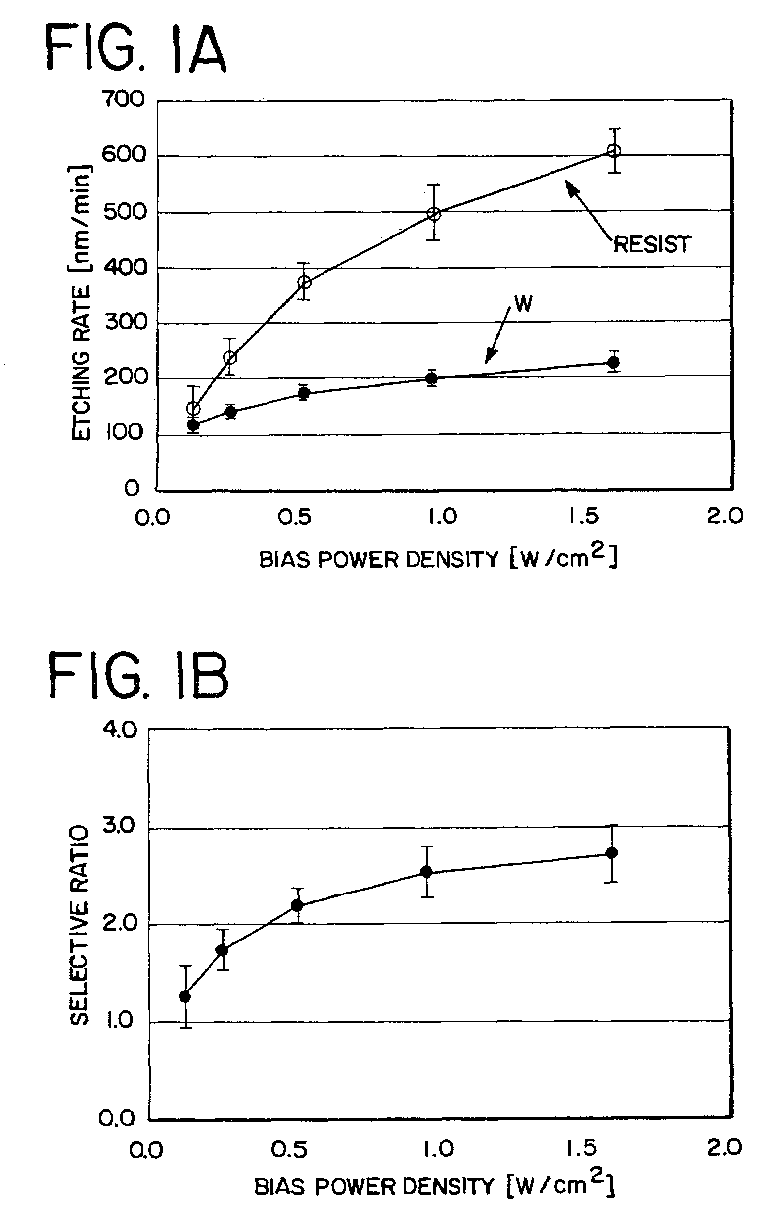
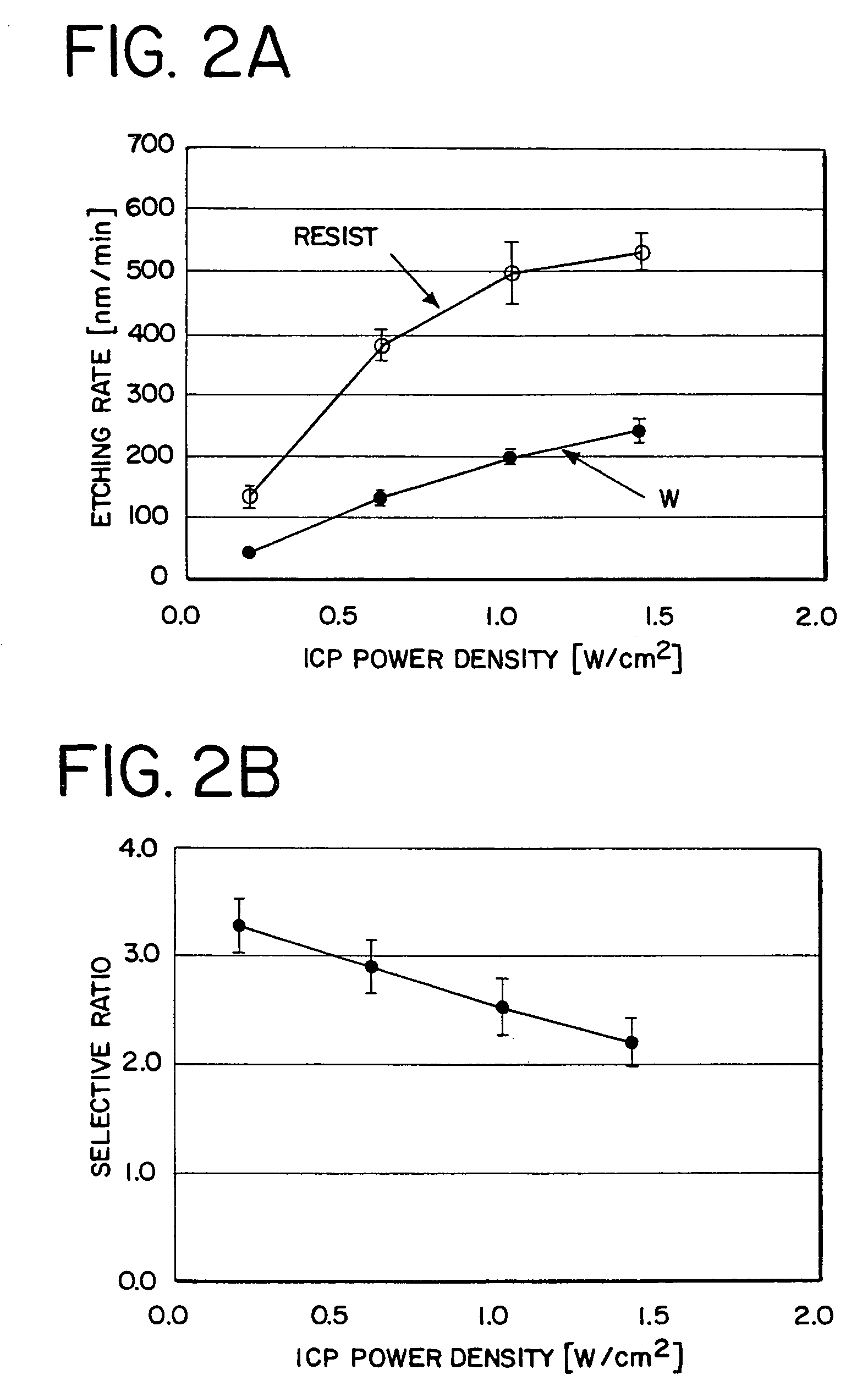
[0089]The present invention employs ICP etching apparatus that uses high-density plasma. The ICP etching apparatus forms plasma through inductive coupling of RF power at a low pressure, thereby obtaining a plasma density of 1011 / cm3 or higher. Using the thus obtained high-density plasma, the apparatus processes at high selective ratio and etching rate.
[0090]First, a detailed description is given on the plasma generating mechanism of ICP dry etching apparatus with reference to FIG. 7A. FIG. 7A is a simplified structural diagram of an etching chamber. A quartz plate 31 is positioned in an upper part of the chamber and an antenna coil 32 is placed on the quartz plate 31. The antenna coil 32 is connected to an RF power supply 34 through a matching box 33. A lower electrode 35 on the substrate side opposite to the antenna coil is connected to another RF power supply 37 through a matching box 36.
[0091]When an RF power is applied to the antenna coil 32 above the substrate, an RF current J ...
embodiment mode 2
[0109]This embodiment gives a description on an experiment in which ICP etching apparatus of multi-spiral coil type described in Embodiment Mode 1 is used to etch a conductive film different from the one in Embodiment Mode 1 while varying etching conditions.
[0110]First, a sample is prepared by forming a conductive film that is an Al—Si (2 wt %) film on a glass substrate by sputtering to a thickness of 500 nm. Then resist is formed and the Al—Si film is etched under etching conditions which include the bias power density, the ICP power density, and the ratio of Cl2 added in the etching and which are varied for each sample. The etching conditions are varied as shown in Table 3. In an evaluation where one etching condition is varied, the other etching conditions are set as shown in Table 4. The bias power and ICP power in Tables 3 and 4 are a value obtained by dividing bias power by an area to which the bias power is applied, 12.5 cm×12.5 cm, and a value obtained by dividing ICP power ...
embodiment 1
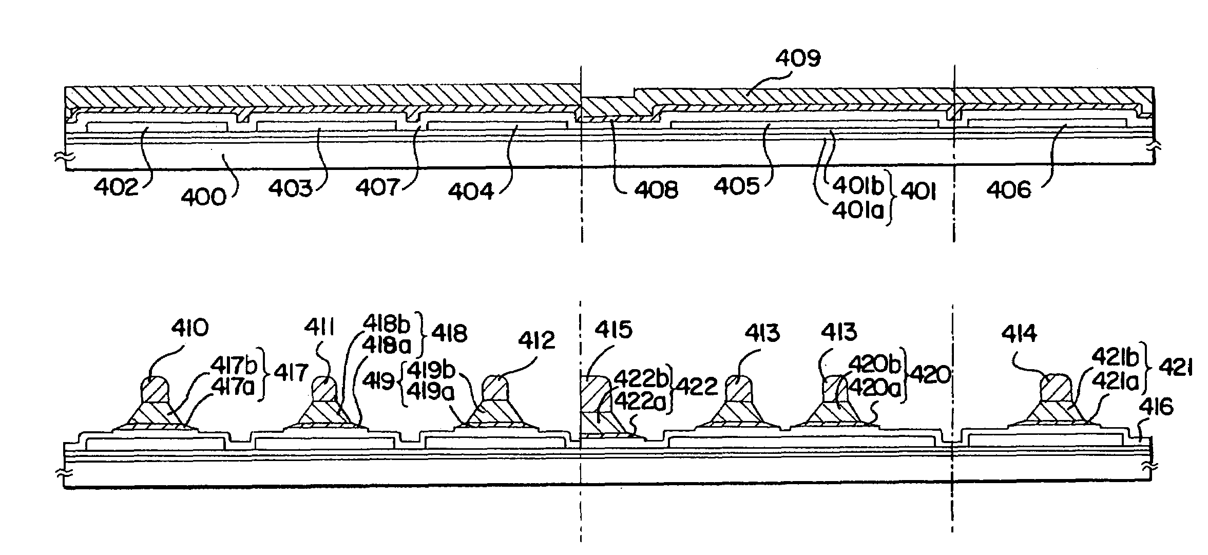
[0118]This embodiment describes with reference to FIGS. 8A to 8C an example of forming a metal wiring that has a tapered portion by controlling parameters involved in etching.
[0119]First, a silicon oxynitride film (composition ratio: Si=32%, O=27%, N=24%, H=17% or composition ratio: Si=32%, O=59%, N=7%, H=2%) with a thickness of 50 nm is formed as an insulating film 11 on a glass substrate 10 by plasma CVD. On the insulating film 11, a TaN film with a thickness of 50 nm is formed as a first conductive film 12 by sputtering. A W film with a thickness of 370 nm is formed as a second conductive film 13 on the first conductive film 12 by sputtering. Then resist (resist 14a) is formed and the W film (the second conductive film 13) is etched while varying the etching conditions including the bias power density, the ICP power density, the pressure, the ratio of oxygen added in the etching, the total flow rate of etching gas, and the temperature of lower electrode. The etching conditions ar...
PUM
| Property | Measurement | Unit |
|---|---|---|
| taper angle | aaaaa | aaaaa |
| temperature | aaaaa | aaaaa |
| pressure | aaaaa | aaaaa |
Abstract
Description
Claims
Application Information
 - R&D
- Intellectual Property
- Life Sciences
- Materials
- Tech Scout
- Unparalleled Data Quality
- Higher Quality Content
- 60% Fewer Hallucinations
Browse by: Latest US Patents, China's latest patents, Technical Efficacy Thesaurus, Application Domain, Technology Topic, Popular Technical Reports.
© 2025 PatSnap. All rights reserved.Legal|Privacy policy|Modern Slavery Act Transparency Statement|Sitemap|About US| Contact US: help@patsnap.com