
System for simplifying layout processing

a layout processing and layout technology, applied in the field of system for simplifying layout processing, to achieve the effect of simplifying and more comprehensive, more complicated and error-pron

Active Publication Date: 2009-02-03
APPLIED MATERIALS INC
View PDF4 Cites 21 Cited by
  • Summary
  • Abstract
  • Description
  • Claims
  • Application Information

AI Technical Summary

Benefits of technology

The present invention provides a layout processing system and method for IC design that addresses issues caused by small jogs or other imperfections in the design. The system uses a preparatory step to create "target" shapes without modifying the original design, followed by a recovery step to correct the design to the original intent. The system can be applied at both the algorithmic and flow levels and can be used with various layout manipulation techniques such as phase-shifting masks. The technical effects of the invention include improved manufacturability of IC designs, simplified application of layout processing, and improved efficiency and accuracy of the design process.

Problems solved by technology

A first processing step (e.g., DRC, process compensation, selective ROPC, etc.) can create jogs, which potentially creates a problem for a second processing step (more than two steps are also possible, where any step before the last step may create jogs, causing a problem for any of the subsequent steps).

Method used


Image

  • System for simplifying layout processing
  • System for simplifying layout processing
  • System for simplifying layout processing

Examples


Embodiment Construction

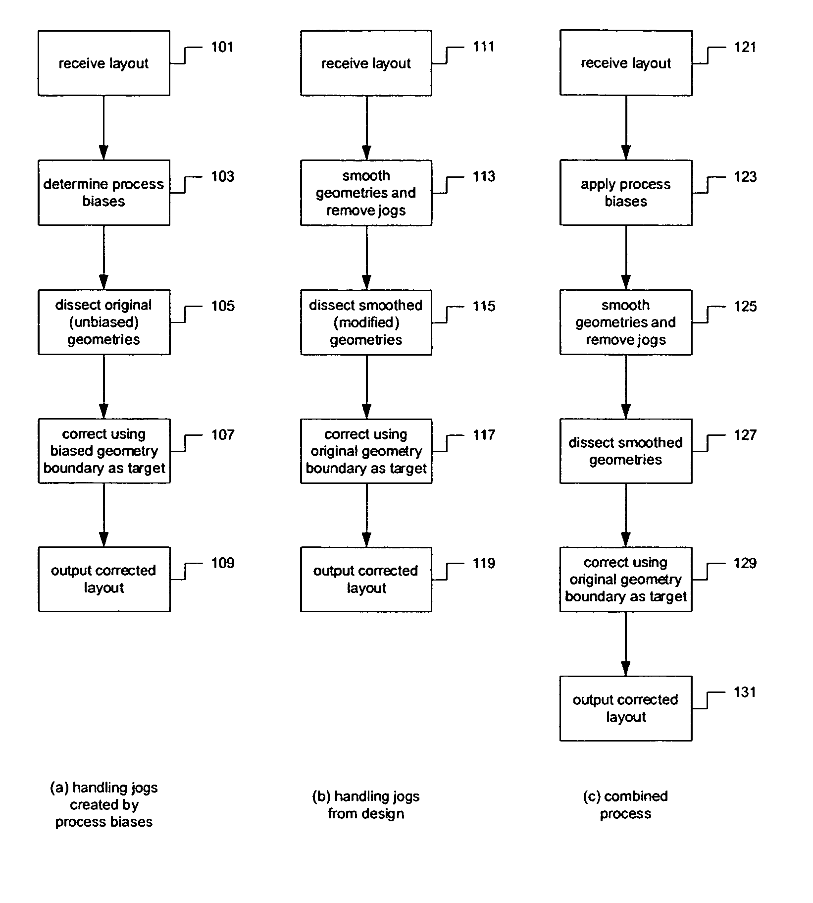
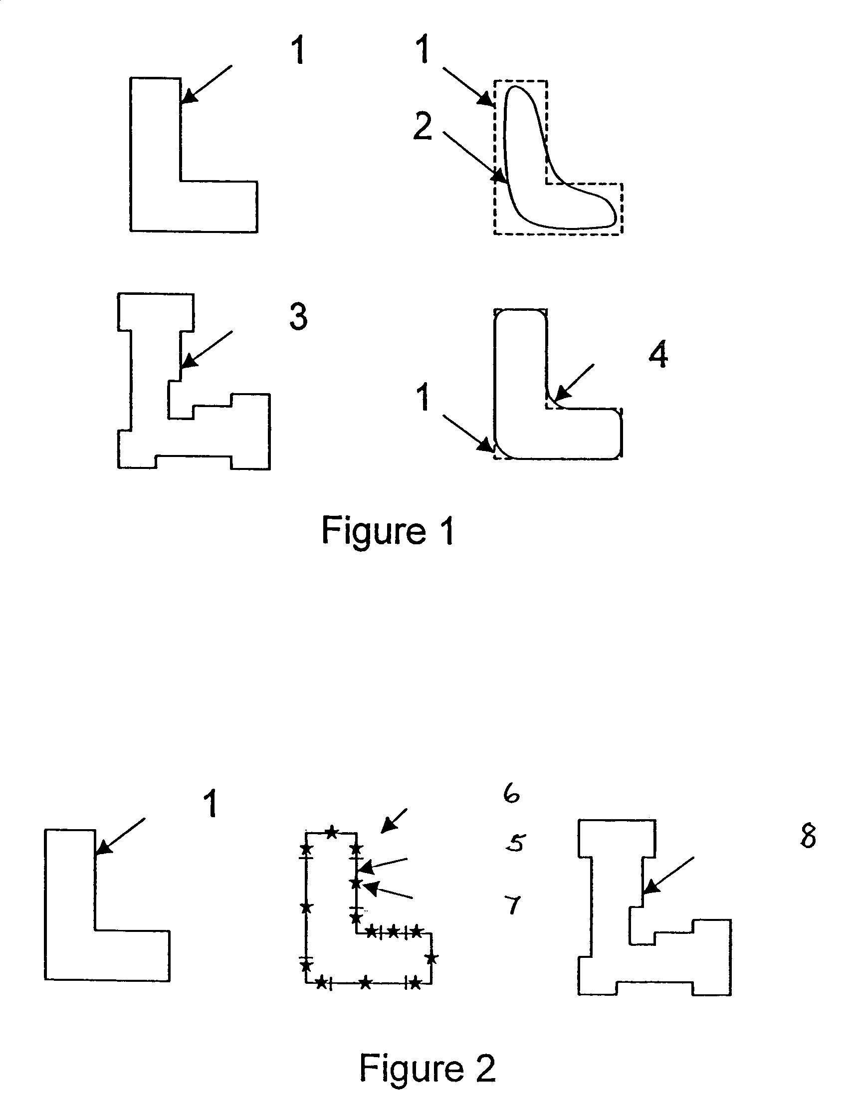
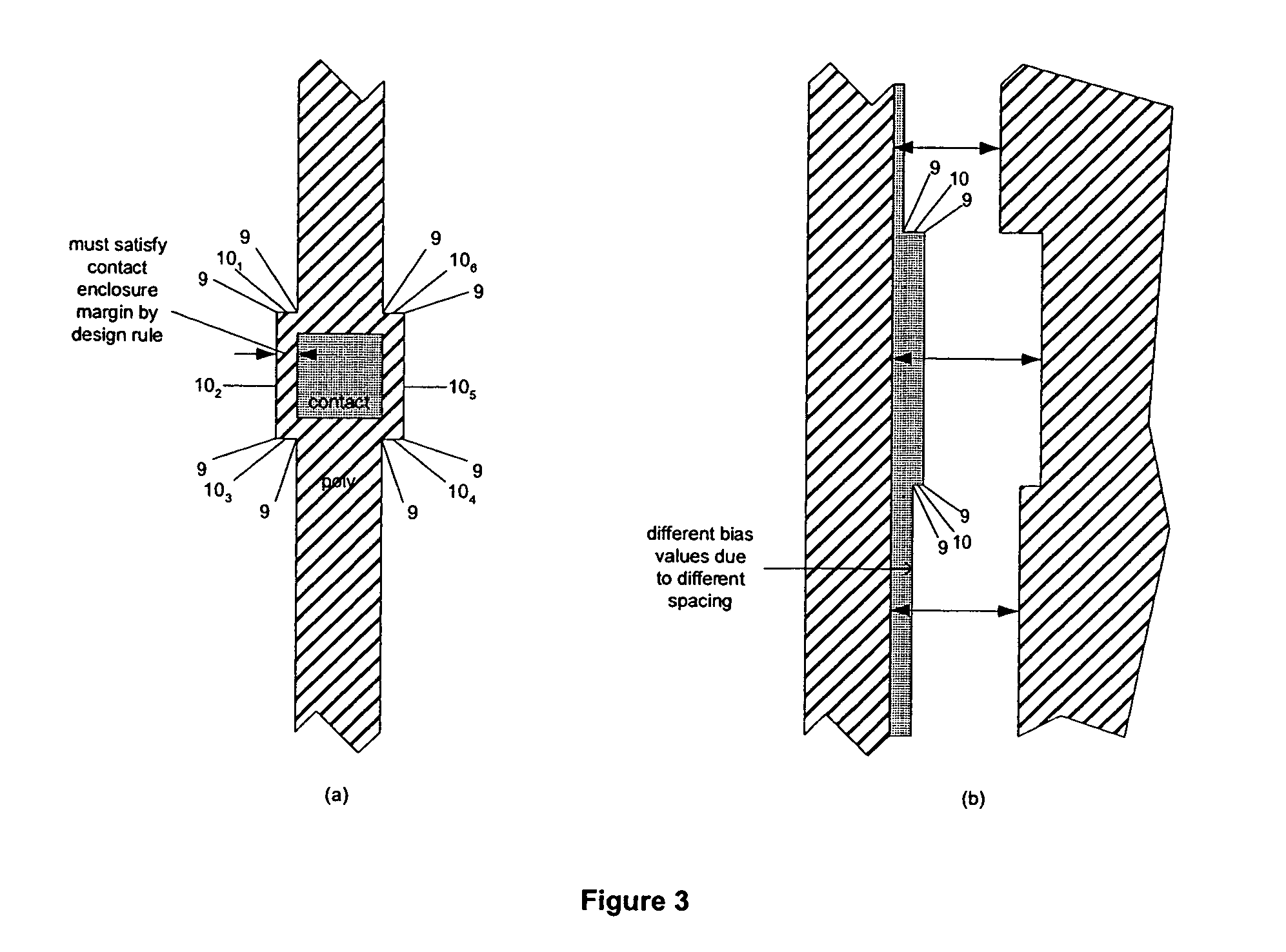
[0055]The present invention is particularly applicable to a computer-implemented software-based IC design layout processing system for generating an IC design based on application of, for example, optical resolution enhancement techniques (RET) such as optical proximity correction (OPC) and phase-shifting masks (PSM) or design rule check (DRC), Boolean or layer operations, or process compensation (e.g., pre-compensation or correction of etch loading effect) to a design layout having or creating imperfections such as jogs, and it is in this context that the various embodiments of the present invention will be described. It will be appreciated, however, that the IC design layout processing system and method in accordance with the various embodiments of the present invention have greater utility, since they may be implemented in hardware or may incorporate other modules or functionality not described herein.

[0056]FIG. 5 is a block diagram illustrating an example of an IC design system ...


PUM


Abstract

A system and method for integrated circuit design are disclosed to enhance manufacturability of circuit layouts by applying layout processing to handle imperfections such as jogs in integrated circuit design layouts. The layout processing may be applied to jogs in the original integrated circuit design layout or jogs created post-design by process biases, as well as design rule check and Boolean processes or process compensation.

Description

CROSS-REFERENCE TO RELATED PATENT APPLICATION[0001]This application relates to U.S. Provisional Patent Application No. 60 / 557,809, filed on Mar. 30, 2004, entitled SYSTEM FOR SIMPLIFYING OPTICAL PROXIMITY CORRECTION DISSECTION USING RETARGET.BACKGROUND OF THE INVENTION[0002]1. Field of the Invention[0003]The present invention relates generally to a system and method for designing integrated circuits or migrating integrated circuit designs from one technology node to another for fabrication by a semiconductor manufacturing process and, more particularly, to a system and method for providing simplified layout processing, for example, optical proximity correction using retarget, for integrated circuit designs to enhance manufacturability and, hence, yield of a semiconductor fabrication process used to produce the integrated circuits.[0004]2. References[0005]U.S. Pat. No. 5,858,580[0006]U.S. Pat. No. 6,430,737 B1[0007]U.S. Pat. No. 6,539,521 B1[0008]U.S. Pat. No. 6,625,801 B1[0009]U.S. ...

Claims


Application Information

Patent Timeline
Patent Type & Authority Patents(United States)
IPC IPC(8): G06F17/50
CPCG06F17/5081G06F2217/12G06F30/398G06F2119/18Y02P90/02
Inventor ZHANG, YOUPINGLAI, WEINONG
Owner APPLIED MATERIALS INC
Learn More