Radio-frequency switching circuit and semiconductor device

a technology of radio frequency switching and semiconductor devices, applied in the direction of electronic switching, semiconductor devices, pulse techniques, etc., can solve the problems of increasing insertion loss, and deterioration of radio frequency characteristics, so as to improve insertion loss, improve frequency characteristics, and efficiently use shunt circuits

Inactive Publication Date: 2009-02-17
PANASONIC CORP
View PDF3 Cites 27 Cited by
  • Summary
  • Abstract
  • Description
  • Claims
  • Application Information

AI Technical Summary

Benefits of technology

[0013]Therefore, an object of the present invention is to provide a radio-frequency switching circuit and a semiconductor device which are capable of improving a frequency characteristic, thereby obtaining favorable insertion loss even at a radio frequency, and also capable of efficiently using a shunt circuit, thereby realizing a high isolation characteristic.
[0021]The above-described present invention allows a stray capacitance value of a transmission path to be reduced at the time of transmission, and allows a stray capacitance value of a reception path to be reduced at the time of reception, thereby obtaining favorable insertion loss even at a radio frequency. Also, according to the present invention, isolation between terminals can be obtained with a small-sized circuit configuration.

Problems solved by technology

However, an antenna switch MMIC structured by FETs has a drawback that a radio-frequency characteristic thereof is deteriorated if a high-power signal is inputted when a power supply voltage is as low as, e.g., 3V.
The increased number of capacitance components causes a deterioration of frequency characteristic, thereby increasing insertion loss.
Also in this case, there is the problem of the deteriorated frequency characteristic caused by the capacitance components of the FETs in off-state.
This causes a problem that frequency dependency becomes great and insertion loss at a radio frequency is increased.
However, when a circuit has a configuration in which a shunt circuit is provided for each terminal, complexity of the configuration of the circuit increases in accordance with an increase in the number of transmission / reception paths.
This causes a problem that a semiconductor chip increases in size.

Method used


Image

  • Radio-frequency switching circuit and semiconductor device
  • Radio-frequency switching circuit and semiconductor device
  • Radio-frequency switching circuit and semiconductor device

Examples


first embodiment

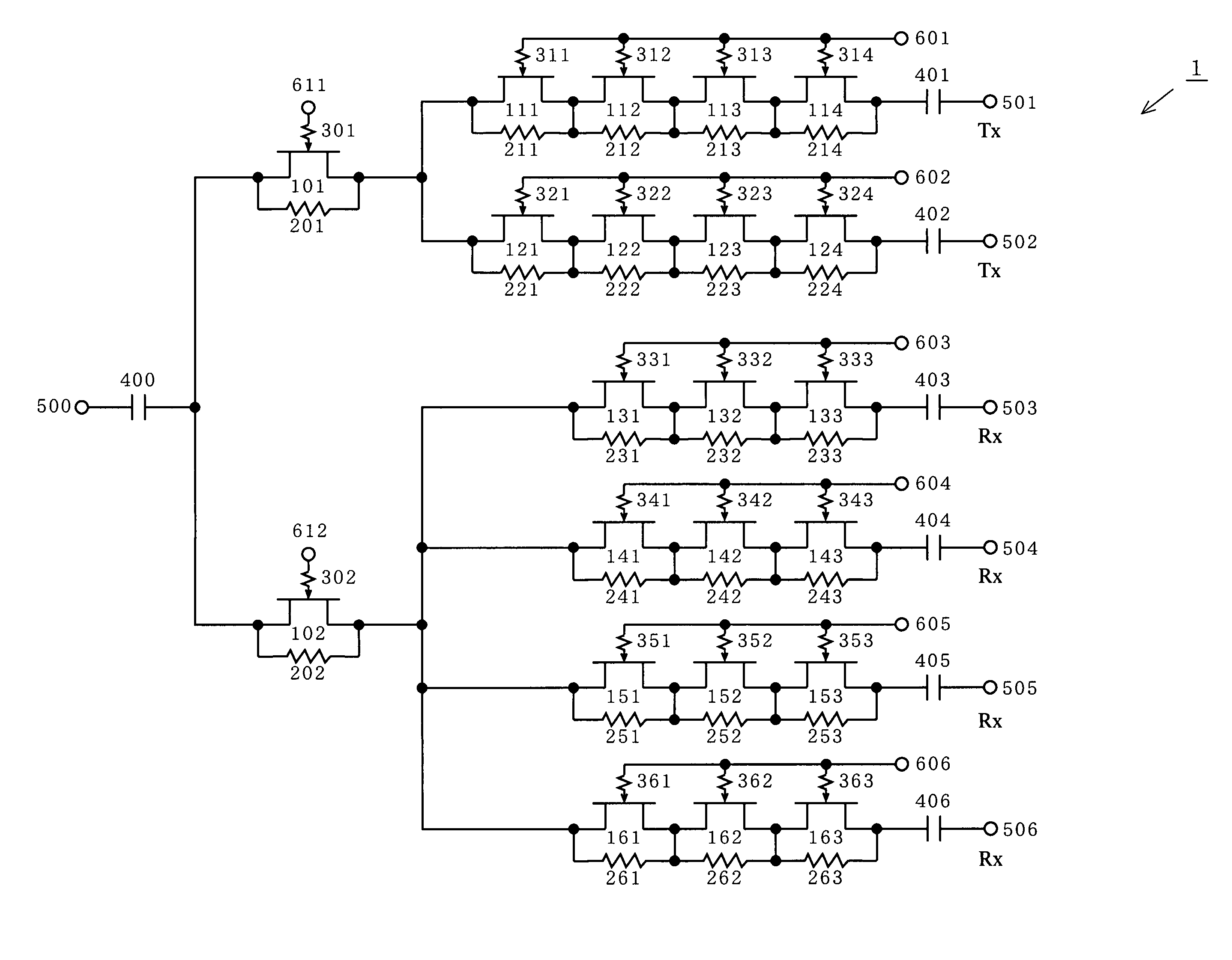
[0046]FIG. 1 shows a configuration of a radio-frequency switching circuit 1 according to a first embodiment of the present invention. The radio-frequency switching circuit 1 comprises: FETs 101, 102, 111 to 114, 121 to 124, 131 to 133, 141 to 143, 151 to 153 and 161 to 163; resistors 201, 202, 211 to 214, 221 to 224, 231 to 233, 241 to 243, 251 to 253, 261 to 263, 301, 302, 311 to 314, 321 to 324, 331 to 333, 341 to 343, 351 to 353 and 361 to 363; capacitors 400 to 406; a common terminal 500; independent terminals 501 to 506; and control terminals 601 to 606, 611 and 612. In the present embodiment, the independent terminals 501 and 502 are transmission terminals TX, and the independent terminal 503 to 506 are reception terminals RX. The FETs are used as switching elements.

[0047]The common terminal 500 is connected to a drain of each of the FETs 101 and 102 via the capacitor 400. The FETs 101 and 102 respectively have drains and sources thereof connected via the resistors 201 and 202...

second embodiment

[0064]FIG. 7 shows a configuration of a radio-frequency switching circuit 2 according to a second embodiment of the present invention. The radio-frequency switching circuit 2 according to the second embodiment comprises: FETs 101 to 104, 111 to 114, 121 to 124, 131, 132, 141, 142, 151, 152, 161 and 162; resistors 201 to 204, 211 to 214, 221 to 224, 231, 232, 241, 242, 251, 252, 261, 262, 301 to 304, 311 to 314, 321 to 324, 331, 332, 341, 342, 351, 352, 361 and 362; capacitors 400 to 406; a common terminal 500; independent terminals 501 to 506; and control terminals 601 to 606 and 611 to 614.

[0065]As shown in FIG. 7, the radio-frequency switching circuit 2 according to the second embodiment has a configuration which is a result of replacing the FETs 133, 143, 153 and 163 and resistors 233, 243, 253, 263, 333, 343, 353 and 363 of the radio-frequency switching circuit 1 according to the first embodiment with the FETs 103 and 104, resistors 203, 204, 303 and 304 and control terminals 61...

third embodiment

[0068]FIG. 8 shows a configuration of a radio-frequency switching circuit 3 according to a third embodiment of the present invention. The radio-frequency switching circuit 3 according to the third embodiment comprises: FETs 101, 102, 111 to 114, 121 to 124, 131 to 133, 141 to 143, 151 to 153 and 161 to 163; resistors 201, 202, 211 to 214, 221 to 224, 231 to 233, 241 to 243, 251 to 253, 261 to 263, 301, 302, 311 to 314, 321 to 324, 331 to 333, 341 to 343, 351 to 353 and 361 to 363; capacitors 400 to 406, 471 and 472; a common terminal 500; independent terminals 501 to 506; and control terminals 601 to 606, 611 and 612.

[0069]As shown in FIG. 8, the radio-frequency switching circuit 3 according to the third embodiment has a configuration which is a result of adding capacitances 471 and 472 as reactance circuits to the radio-frequency switching circuit 1 according to the first embodiment. Since a fundamental function and effect of the radio-frequency switching circuit 3 are same as thos...


PUM


Abstract

A common terminal 500 is connected to drains of FETs 101 and 102 via a capacitor 400. FETs 111 to 114 are serially connected, and inserted between a source of the FET 101 and a terminal 501 via a capacitor 401. Similarly, each of: FETs 121 to 124; FETs 131 to 133; FETs 141 to 143; FETs 151 to 153; and FETs 161 to 163 is inserted between the source of the FET 101 or an FET 102 and a corresponding one of terminals 502 to 506. This configuration allows a stray capacitance value of a transmission / reception path to be reduced at the time of transmission / reception, thereby obtaining a favorable radio-frequency characteristic.

Description

BACKGROUND OF THE INVENTION[0001]1. Field of the Invention[0002]The present invention relates to a radio-frequency switching circuit and a semiconductor device, and particularly to a radio-frequency switching circuit used for, e.g., a multi-band communication device compatible with a plurality of frequency bands, and a semiconductor device having a semiconductor substrate on which the radio-frequency switching circuit is integrated.[0003]2. Description of the Background Art[0004]In recent years, there has been a demand for mobile communication devices such as cellar phones to be decreased in size and improve in performance. In order to meet such a demand, Antenna Switch MMIC technology has been proposed in which a field-effect transistor (hereinafter, referred to as FET) using gallium arsenide (GaAs) is used as a signal path switching element such as an antenna.[0005]However, an antenna switch MMIC structured by FETs has a drawback that a radio-frequency characteristic thereof is de...

Claims


Application Information

Patent Timeline
Patent Type & Authority Patents(United States)
IPC IPC(8): H01P1/10H01P1/15H03H11/34
CPCH01P1/15H03K17/002H03K17/063H03K17/102H03K17/693
Inventor NAKATSUKA, TADAYOSHISUWA, ATSUSHINAKAGAWA, MOTOOADACHI, MASAKAZU
Owner PANASONIC CORP
Why Eureka
Try Eureka