Ternary nitride-based buffer layer of a nitride-based light-emitting device and a method for manufacturing the same

a technology of nitride-based light-emitting devices and buffer layers, which is applied in the direction of polycrystalline material growth, protective switch terminals/connections, crystal growth processes, etc., can solve the problems of complex and difficult production process, inability to efficiently reduce the dislocation density, and affect the quality of prior art nitride-based light-emitting devices, etc., to reduce the production duration of heating and simplify the production process. , the effect of reducing

Active Publication Date: 2009-03-03
EPISTAR CORP
View PDF9 Cites 4 Cited by
  • Summary
  • Abstract
  • Description
  • Claims
  • Application Information

AI Technical Summary

Benefits of technology

[0008]The present invention method can simplify the complex and difficult production process and decrease the production duration of heating and cooling as well as re-crystallization processes. The present invention can select Ga as the second group III element according to the production process, so as to proceed to grow the high-temperature GaN layer after forming the first group III element transient layer, where the ternary nitride-based buffer layer can be formed naturally without any special treatment, so that the production process can be simplified, and the quality of epitaxy film can be increased. Meanwhile, the cost of production can be decreased.

Problems solved by technology

Due to problems associated with the matching of crystal lattice constants, dislocation density (which affects quality of the prior art nitride-based light-emitting device), cannot be decreased efficiently.
The thickness and temperature of the buffer layer, recovery of the heating and re-crystallization processes, plus the ratio and flow rate of gas for each reaction must be controlled precisely, thus making the production process complex and difficult, and as a consequence production efficiency cannot be increased.

Method used


Image

  • Ternary nitride-based buffer layer of a nitride-based light-emitting device and a method for manufacturing the same
  • Ternary nitride-based buffer layer of a nitride-based light-emitting device and a method for manufacturing the same
  • Ternary nitride-based buffer layer of a nitride-based light-emitting device and a method for manufacturing the same

Examples


Embodiment Construction

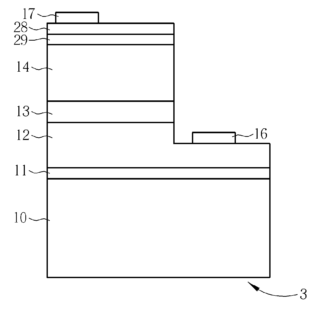
[0017]Please refer to FIG. 1, which illustrates a schematic diagram of a present invention nitride-based light-emitting device 1 with an AlGaN buffer layer. The nitride-based light-emitting device 1 includes a sapphire substrate 10, an AlGaN buffer layer 11 formed over the sapphire substrate 10, an n-type nitride-based semiconductor stack layer 12 formed over the AlGaN buffer layer 11 with an epitaxy area 121 and an n-type electrode contact area 122, a GaN / InGaN multi-quantum well light-emitting layer 13 formed over the epitaxy area 121, a p-type nitride-based semiconductor stack layer 14 formed over the GaN / InGaN multi-quantum well light-emitting layer 13, a metal transparent conductive layer 15 formed over the p-type nitride-based semiconductor stack layer 14, an n-type electrode 16 formed over the n-type electrode contact area 122, and a p-type electrode 17 formed over the metal transparent conductive layer 15.

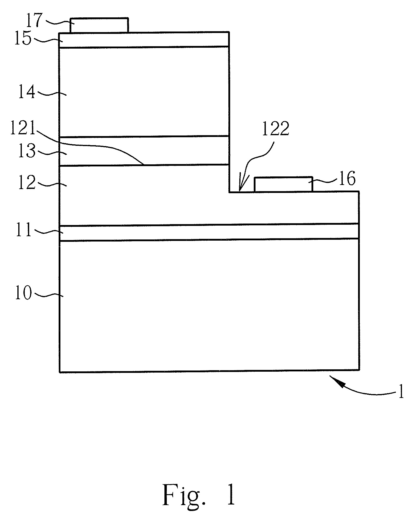
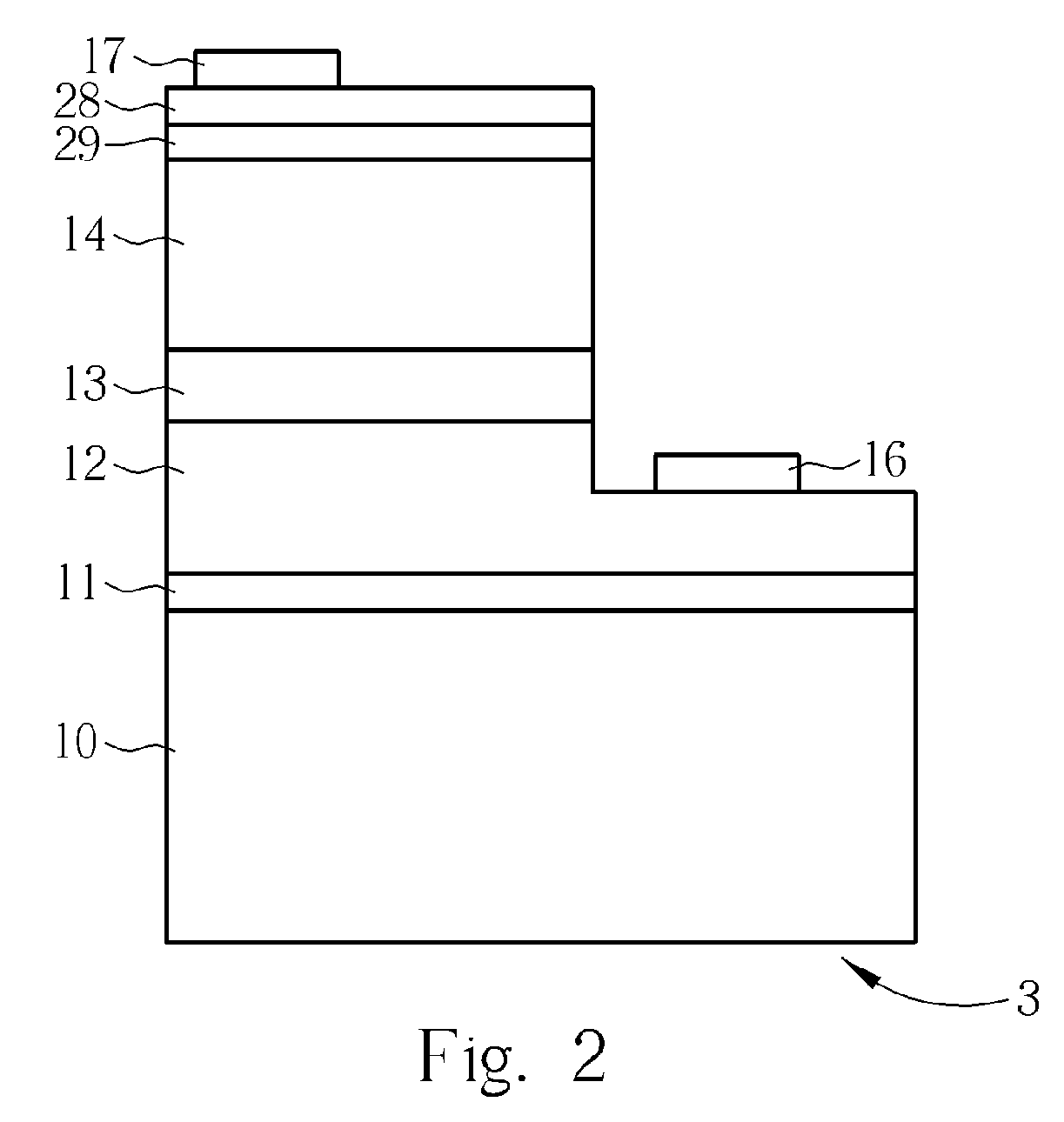
[0018]A method for forming the above-mentioned AlGaN buffer layer of t...


PUM

PropertyMeasurementUnit
temperatureaaaaaaaaaa
thicknessaaaaaaaaaa

Abstract

Ternary nitride-based buffer layer of a nitride-based light-emitting device and related manufacturing method. The device includes a substrate and a plurality of layers formed over the substrate in the following sequence: a ternary nitride-based buffer layer, a first conductivity type nitride-based semiconductor layer, a light-emitting layer, and a second conductivity type nitride-based semiconductor layer. The manufacturing method includes introducing a first reaction source containing a first group III element into a chamber at a first temperature that is subsequently deposited on the surface of the substrate, the melting point of said element being lower than the first temperature. Introducing a second reaction source containing a second group III element and a third reaction source containing a nitrogen element into the chamber at a second temperature, no lower than the melting point of the first group III element, for forming a ternary nitride-based buffer layer with the first group III element.

Description

BACKGROUND OF THE INVENTION[0001]1. Field of the Invention[0002]The present invention provides a nitride-based light-emitting device and a method for manufacturing the same, and more particularly, a nitride-based light-emitting device with a ternary nitride-based buffer layer.[0003]2. Description of the Prior Art[0004]The applications of light-emitting diodes are extensive and include optical display devices, traffic signals, data storing devices, communication devices, illumination devices, and medical apparatuses. As such, it is important to increase the brightness of light-emitting diodes, and to simplify manufacturing processes in order to decrease the cost of the light-emitting diode.[0005]In general, a prior art nitride-based light-emitting device includes a nitride-based buffer layer of group AlGalnN formed over a sapphire substrate, and undergoes a nitride-based epitaxy process on the nitride-based buffer layer. Due to problems associated with the matching of crystal lattice...

Claims


Application Information

Patent Timeline
Patent Type & Authority Patents(United States)
IPC IPC(8): C30B25/02H01L21/00H01L21/20H01L21/205H01L33/06H01L33/12H01L33/32
CPCH01L33/007H01L21/0237H01L21/0242H01L21/0254H01L21/0262H01L21/02458H01H71/08
Inventor OU, CHENLIN, WEN-HSIANGLAI, SHIH-KUO
Owner EPISTAR CORP
Why Eureka
Try Eureka