

Solid state imaging device including annular and center lens in contact with each other
a technology of solid-state imaging and annular lenses, which is applied in the field of solid-state imaging devices, can solve problems such as color intermixing, and achieve the effects of reducing color intermixing, reducing size, and improving sensitivity
- Summary
- Abstract
- Description
- Claims
- Application Information
AI Technical Summary
Benefits of technology
Problems solved by technology
Method used
Image

Examples
first embodiment
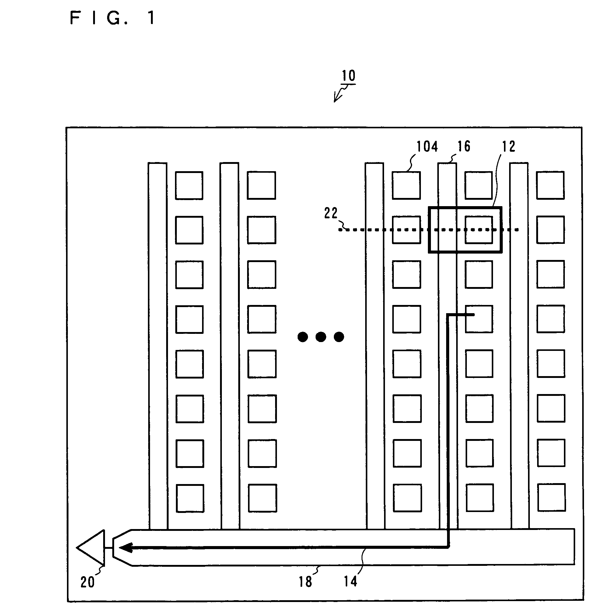
[0035]FIG. 1 is a schematic plan view showing a solid-state imaging device according to a first embodiment of the present invention. FIG. 1 mainly shows features involved in charge transfer. The solid-state imaging device includes a plurality of pixels. In FIG. 1, an area occupied by a single pixel is represented as a unit pixel 12. Photodiode sections 104, which function as photoelectric conversion sections, generate electrical charges in accordance with the intensity of the light received thereby. Each vertical CCD 16 receives from a plurality of pixels the electrical charges generated by the respective photodiode sections 104, and transfers the electrical charges. A horizontal CCD 18 receives the electrical charges from the vertical CCDs 16, and transfers the electrical charges to an output amplifier 20. A flow of the signal charge is indicated by an arrow 14.
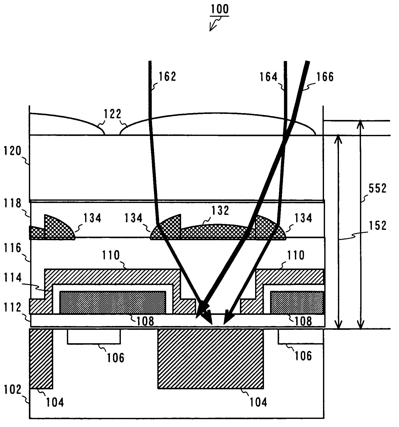
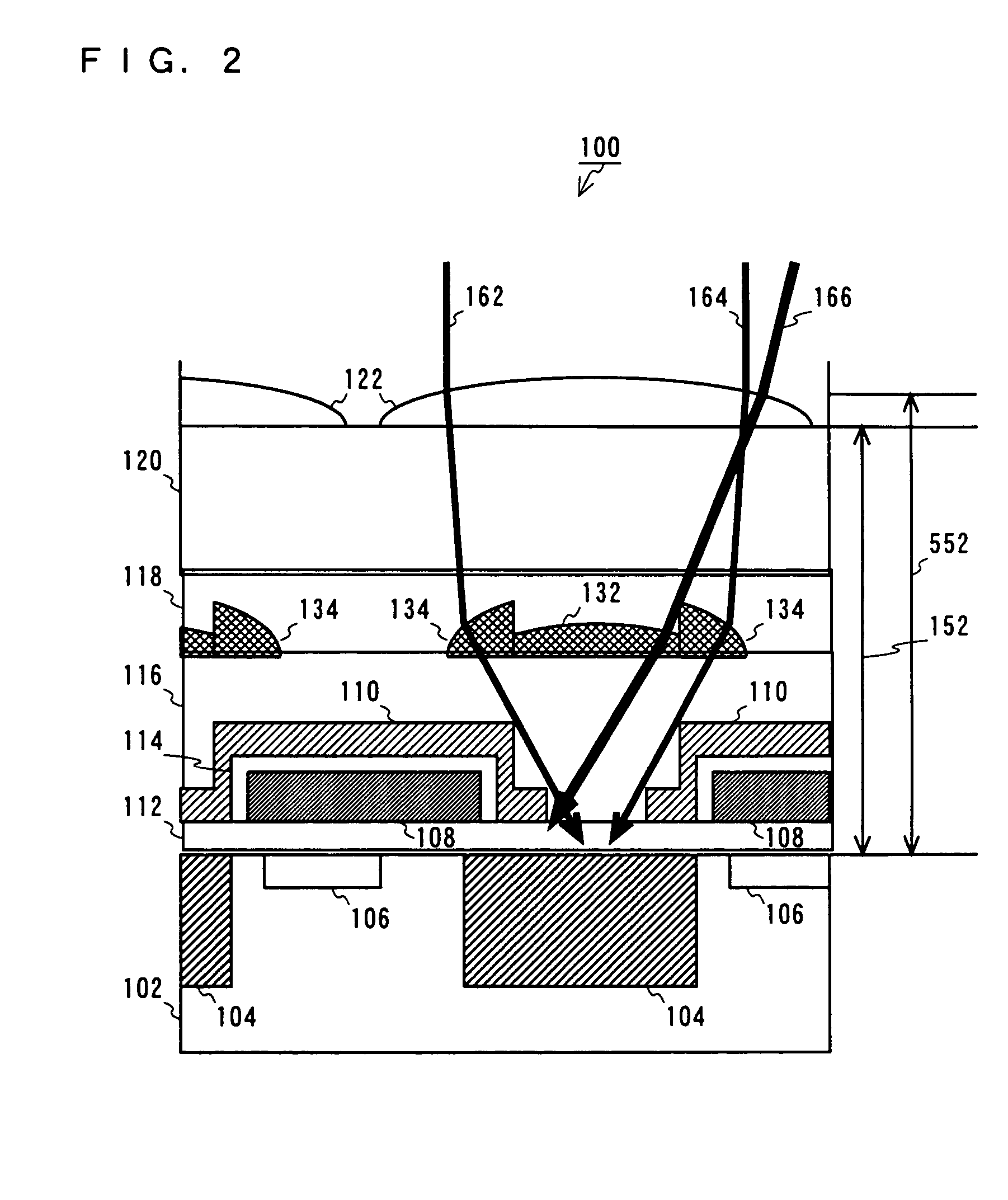
[0036]FIG. 2 is a schematic cross-sectional view showing the solid-state imaging device according to the first embodiment,...
second embodiment
[0057]FIG. 9 is a schematic cross-sectional view showing a solid-state imaging device according to a second embodiment of the present invention. Hereinafter, the second embodiment of the present invention will be described with reference to FIG. 9. Although the present embodiment illustrates an interline CCD solid-state imaging device, the present invention is also applicable to any other type of solid-state imaging device, e.g., a MOS-type solid-state imaging device.
[0058]As shown in FIG. 9, the solid-state imaging device according to the present embodiment includes an Si substrate 102, photodiode sections 104, charge transfer sections 106, gate electrodes 108, a photoshield metal film 110, a MOS gate insulative film 112, an interlayer insulative film 114, an insulative film 116, upper lenses 122, and a color filter 120, which are identical to their respective counterparts in the first embodiment. The descriptions of such features will be omitted.
[0059]In the present embodiment, ea...
third embodiment
[0069]The first and second embodiments illustrated solid-state imaging devices of an interline CCD type. However, the solid-state imaging device according to the present invention may be any other CCD-type solid-state imaging device or a MOS-type imaging device. FIGS. 16 and 17 are schematic cross-sectional views each illustrating a case where a MOS imaging device of an FDA (Floating Diffusion Amp) type is adopted as the solid-state imaging device. The present embodiment is similarly applicable to any other MOS-type solid-state imaging device.
[0070]In the case of an MOS-type imaging device, in particular, multiple layers of wiring are generally employed. Therefore, in order to allow light from an external source to be efficiently converged to the photodiode sections, it is preferable to employ multiple layers of lenses. By adopting a Fresnel lens structure for the intralayer lenses, as shown in FIGS. 16 and 17, the height of the intralayer lenses can be made lowered than the thickne...
PUM
 Abstract
Description
Claims
Application Information