Planar antenna structure and radio device

Active Publication Date: 2009-03-10
CANTOR FITZGERALD SECURITIES
View PDF28 Cites 51 Cited by
  • Summary
  • Abstract
  • Description
  • Claims
  • Application Information

AI Technical Summary

Benefits of technology

[0008]An advantage of the invention is that the radiating element need not be shaped in order to provide resonating frequencies or antenna matching. Instead, it can be designed relatively freely based on the desired external appearance of the device, for example. Another advantage of the invention is that the antenna needs relatively little space inside the device. This is based on the fact that the distance of the radiator from the ground plane can be considerably smaller than in a corresponding PIFA. A further advantage of the invention is that when the radiating element is located in / on the cover of the device, the radiating characteristics of the antenna are better compared to a radiator located more inwardly. A further advantage of the invention is that the production costs of the antenna according to the invention are relatively low.
is that the radiating element need not be shaped in order to provide resonating frequencies or antenna matching. Instead, it can be designed relatively freely based on the desired external appearance of the device, for example. Another advantage of the invention is that the antenna needs relatively little space inside the device. This is based on the fact that the distance of the radiator from the ground plane can be considerably smaller than in a corresponding PIFA. A further advantage of the invention is that when the radiating element is located in / on the cover of the device, the radiating characteristics of the antenna are better compared to a radiator located more inwardly. A further advantage of the invention is that the production costs of the antenna according to the invention are relatively low.

Problems solved by technology

A disadvantage of the structure shown in FIG. 1 is that when trying to achieve a very small device, the space required by the radiating plane within the device may be too big.
This, however, would restrict the design of the radiating element and thus make it more difficult to achieve the electrical characteristics desired.
Furthermore, such an antenna structure would have only one operating band, which would be a disadvantage.

Method used


Image

  • Planar antenna structure and radio device
  • Planar antenna structure and radio device
  • Planar antenna structure and radio device

Examples


Embodiment Construction

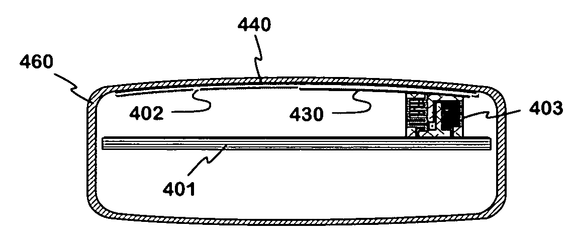
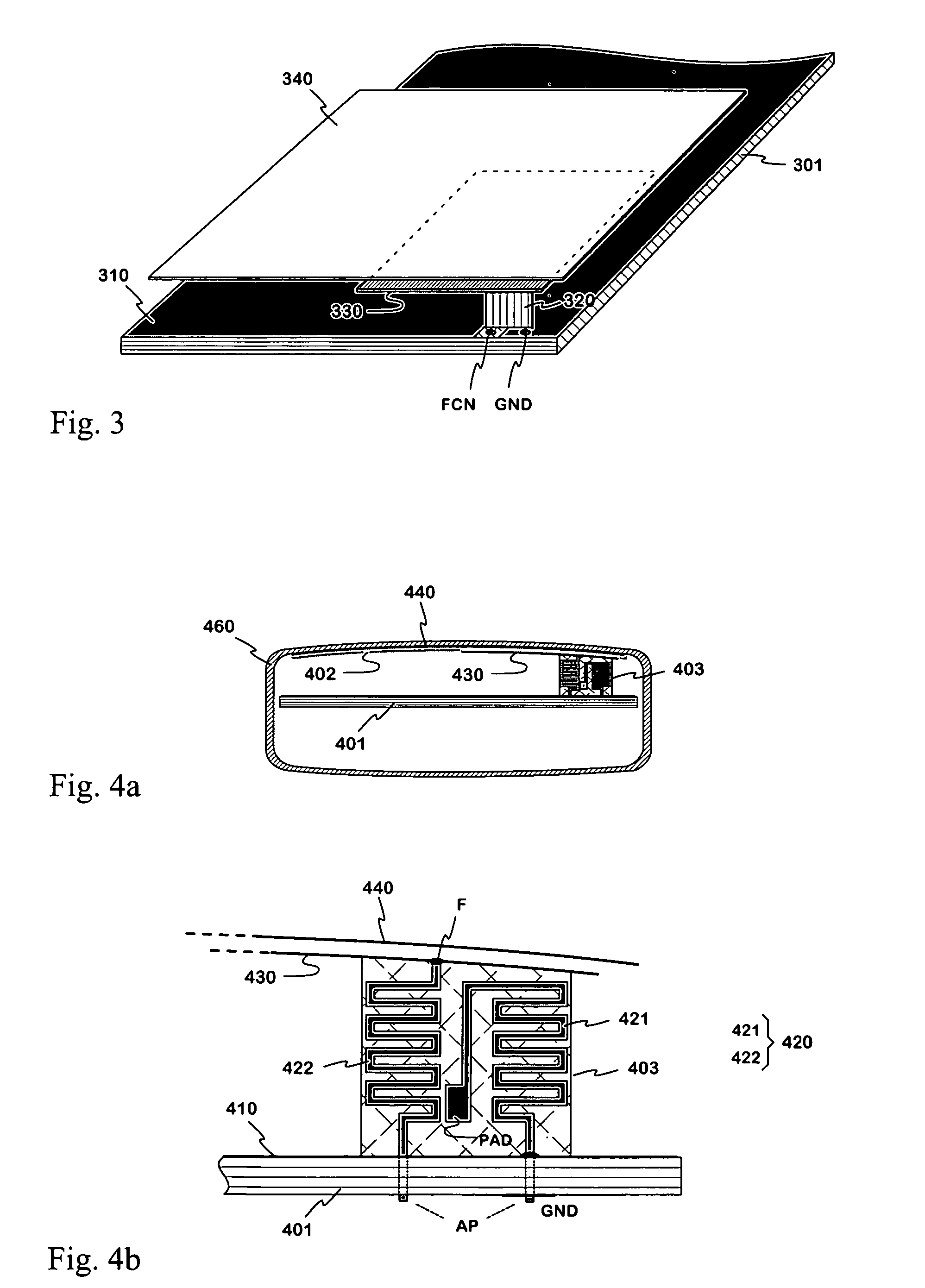
[0016]FIG. 3 illustrates the principle of the planar antenna structure according to the invention. In the figure there is seen a circuit board 301 of a radio device, the conductive upper surface of the circuit board serving as signal ground and ground plane 310 for the antenna. Above the ground plane there is a parallel planar radiating element 340. Between the ground plane and radiating element, clearly closer to the latter than the former, there is a planar feed element 330. Its size is a fraction of the size of the radiating element. Between the radiating element and feed element exists only an electromagnetic coupling.

[0017]The antenna structure depicted in FIG. 3 further includes a feed circuit 320 which connects the feed element 330 to the antenna port of the radio device. The antenna port, in turn, is in connection with the transmitter and receiver in the radio device. The feed circuit has a galvanic contact to the signal ground GND. The antenna feed conductor comes from the ...


PUM


Abstract

A planar antenna structure intended to be used in small portable radio devices and a radio device using an antenna structure according to the invention. The radiating element (340) of the antenna is a conductive part in the cover of the radio device or a conductive coating attached to the cover. The radiating element is fed electro-magnetically by a parallel planar feed element (330) connected to the antenna port and located near the radiating element, between it and the ground plane (310). Between the feed element and antenna port there is a feed circuit (320) to provide matching for the antenna and, if necessary, forming an additional operating band. The radiating element need not be shaped to set the resonating frequencies or match the antenna. Instead, it can be designed relatively freely, based on the desired external appearance of the device, for example. Moreover the antenna requires relatively little space within the device.

Description

[0001]The invention relates in particular to a planar antenna structure intended to be used in small portable radio devices. The invention also relates to a radio device having an antenna according to the invention.BACKGROUND OF THE INVENTION[0002]In portable radio devices, mobile communication devices in particular, the antenna is preferably located within the covers of the device for user convenience. An internal antenna of a small-sized device is usually a planar type antenna because in that case it is easiest to achieve an antenna with satisfactory electrical characteristics. A planar antenna includes a radiating plane and a ground plane parallel thereto. FIG. 1 shows an example of a known internal planar antenna with its feed arrangement. Depicted in the figure there is a circuit board 101 of a radio device, which circuit board has a conductive upper surface. This conductive surface serves as a ground plane 110 in the planar antenna. At one end of the circuit board there is the...

Claims


Application Information

Patent Timeline
IPC IPC(8): H01Q1/38H01Q1/24H01Q5/00H01Q5/335H01Q9/04H01Q19/00
CPCH01Q1/243H01Q1/38H01Q9/0414H01Q5/335H01Q9/0442H01Q9/0457H01Q19/005H01Q9/0421
Inventor MIKKOLA, JYRKI
Owner CANTOR FITZGERALD SECURITIES
Why Eureka
Try Eureka