Memory replacement mechanism in semiconductor device

a memory replacement and semiconductor technology, applied in the direction of memory adressing/allocation/relocation, instruments, climate sustainability, etc., can solve the problems of increasing the number of memories mounted, the difficulty of memory replacement, so as to reduce the amount of memory transfer necessary for memory replacement and reduce power consumption.

Inactive Publication Date: 2009-03-10
SOCIONEXT INC
View PDF11 Cites 2 Cited by
  • Summary
  • Abstract
  • Description
  • Claims
  • Application Information

AI Technical Summary

Benefits of technology

[0027]It is therefore an object of the present invention to solve the foregoing conventional problems and achie

Problems solved by technology

In a conventional memory-mounted processor, the scaling up of a program mounted thereon leads directly to an increase in the quantity of memories mounted thereon so that the problems of higher cost and a lower operating speed are encountered.
However, the foregoing conventiona

Method used


Image

  • Memory replacement mechanism in semiconductor device
  • Memory replacement mechanism in semiconductor device
  • Memory replacement mechanism in semiconductor device

Examples


Embodiment Construction

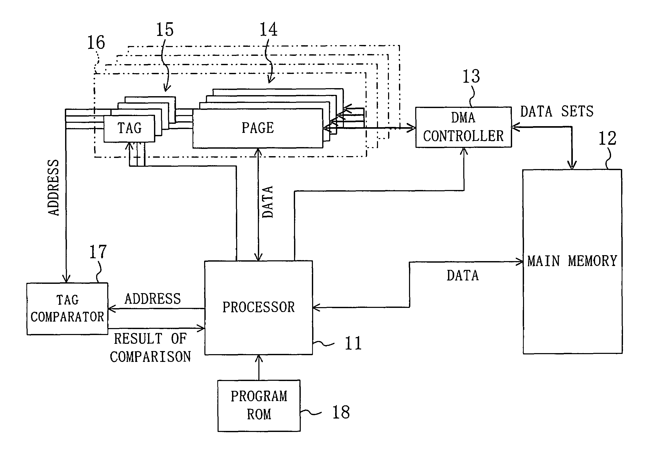
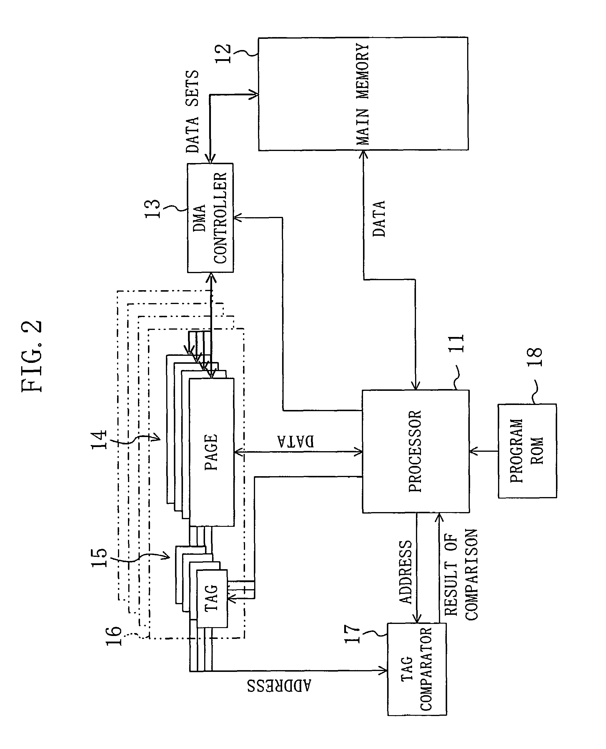
[0072]A description will be given first to terminology used in the embodiments of the present invention.

[0073](1) Pseudo-Cache

[0074]A pseudo-cache memory is composed of a plurality of pages each having a capacity of several kilobytes, which is different from a conventional cache memory composed of a plurality of lines each having a capacity of about several tens of bytes. The pseudo-cache is composed of a memory device accessible at a high speed. The pseudo-cache is preferably composed of, e.g., a static random access memory (SRAM) or the like having a relatively small capacity.

[0075](2) Page

[0076]A page is a smallest unit of a memory region. A tag required to implement the pseudo-cache memory is allocated to each page in a one-to-one correspondence. The mapping of a main memory space to a pseudo-cache space can be performed on a per page basis.
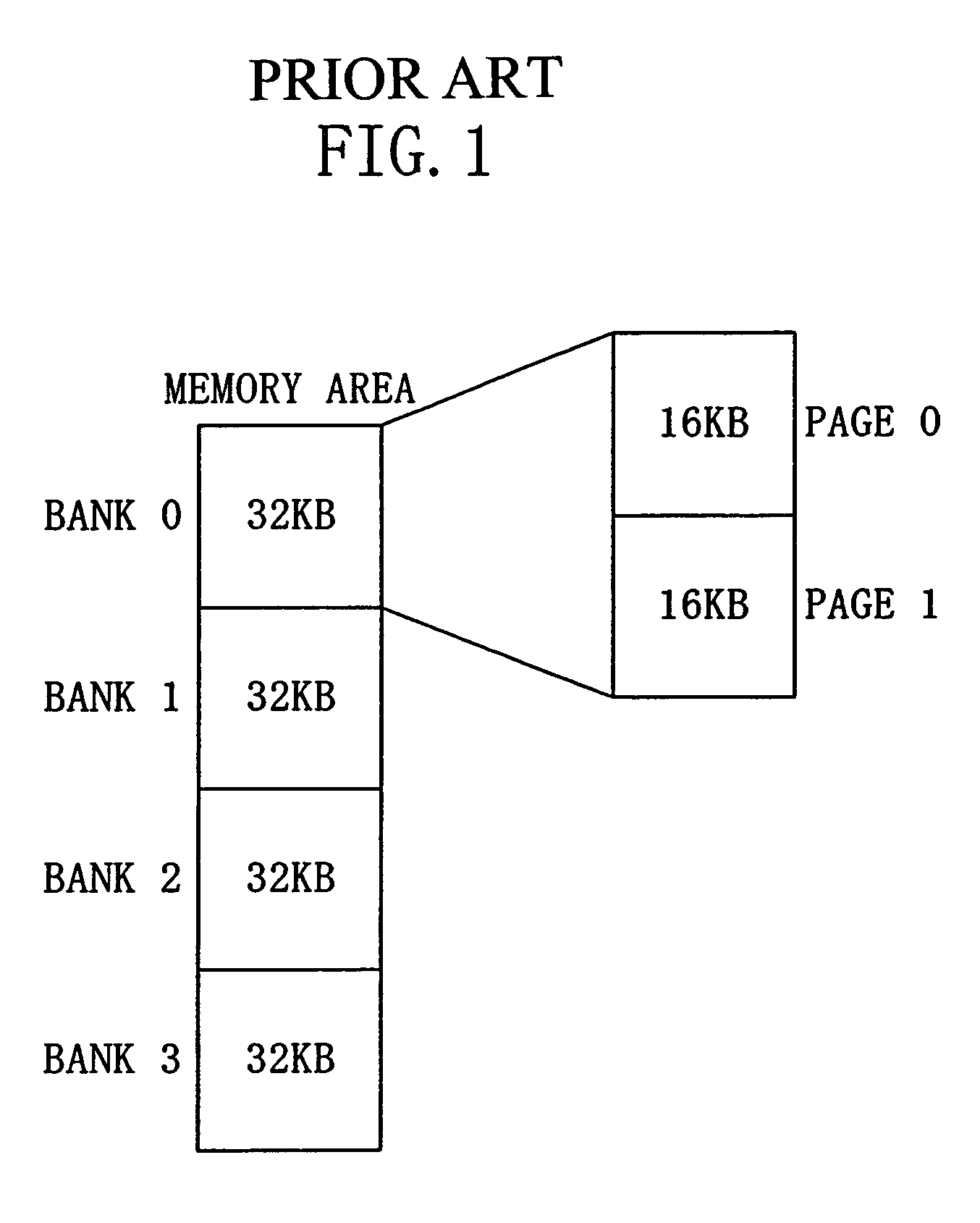
[0077](3) Bank

[0078]A bank is composed of a plurality of pages. The issue of an instruction from a processor to different banks or an access...


PUM


Abstract

A semiconductor device has a processor, a first memory unit accessed by the processor, a plurality of page memory units obtained by partitioning a second memory unit which is accessible by the processor at a speed higher than the speed at which the first memory unit is accessible such that each of the page memory units has a storage capacity larger than the memory capacity of a line composing a cache memory, a tag adding, to each of the page memory units, tag information indicative of an address value in the first memory unit and priority information indicative of a replacement priority, a tag comparator for comparing, upon receipt of an access request from the processor, the address value in the first memory unit with the tag information held by the tag, and a replacement control unit for replacing the respective contents of the page memory units.

Description

BACKGROUND OF THE INVENTION[0001]The present invention relates to a semiconductor device having a processor, in a broad sense, with a memory replacement mechanism.[0002]In a conventional memory-mounted processor, the scaling up of a program mounted thereon leads directly to an increase in the quantity of memories mounted thereon so that the problems of higher cost and a lower operating speed are encountered.[0003]To solve the problems, there has been proposed a structure provided with a memory replacement mechanism in which a low-cost large-scale memory is used to compose a main memory irrespective of the low-speed operation thereof and small-capacity memories are mounted on a processor. In the structure, a program is executed by performing replacement between the small-capacity memories and the main memory. It has been a main stream to use so-called cache memories for such a conventional memory replacement mechanism.[0004]A description will be given herein below to a conventional b...

Claims


Application Information

Patent Timeline
IPC IPC(8): G06F12/00G06F12/12
CPCG06F12/121Y02B60/1225Y02D10/00
Inventor KOGA, YOSHIHIROKURODA, MANABUASAI, NOBORUFUNAHASHI, KAZUTOSHI
Owner SOCIONEXT INC
Why Eureka
Try Eureka