Non-volatile memory cell circuit with programming through band-to-band tunneling and impact ionization gate current

a non-volatile memory and gate current technology, applied in static storage, digital storage, instruments, etc., can solve the problems of insufficient qb>1/b>, insufficient amount of high-energy electrons, and inability to control these transport mechanisms

Active Publication Date: 2009-03-24
SYNOPSYS INC
View PDF10 Cites 26 Cited by
  • Summary
  • Abstract
  • Description
  • Claims
  • Application Information

AI Technical Summary

Problems solved by technology

With the ever decreasing size of transistor dimensions (e.g., in terms of gate length and gate dielectric thickness), however, the ability to control these transport mechanisms is proving to be increasingly difficult.
In this case, transistor Q1 is not sufficiently “on” and, as a consequence, an insufficient amount of high energy electrons are created and injected onto the floating gate 101.
The result is that the first logical state cannot be reached in time.

Method used


Image

  • Non-volatile memory cell circuit with programming through band-to-band tunneling and impact ionization gate current
  • Non-volatile memory cell circuit with programming through band-to-band tunneling and impact ionization gate current
  • Non-volatile memory cell circuit with programming through band-to-band tunneling and impact ionization gate current

Examples


Embodiment Construction

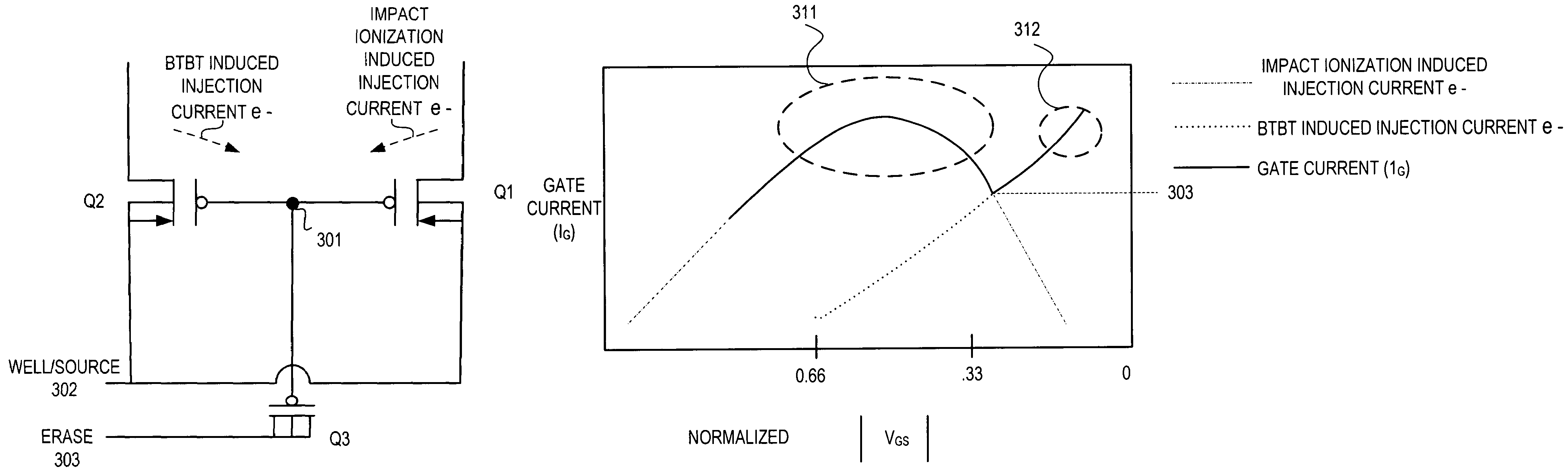
[0033]FIG. 3A shows a circuit diagram for an improved non volatile memory cell that avoids the problems described above with respect to the prior art circuit of FIG. 1. FIG. 3B graphically depicts a possible design point for the circuit of FIG. 3A that is directly comparable to FIG. 2.

[0034]Referring to FIG. 3A, transistor Q1 and the Fowler-Nordheim tunneling transistor Q3 (noting that reference Q2 was used for the tunneling transistor with reference to FIG. 1) operate as described above with respect to FIG. 1. That is, during a PROGRAM phase, high energy electrons (created from lattice collisions with carriers accelerated in Q1's conductive channel) are supposed to be injected to the floating gate 301 from the substrate portion of transistor Q1 thereby lowering the floating gate 301 charge level and corresponding voltage to a first logical state. Moreover, during an ERASE phase, electrons are removed from the floating gate 301 by Fowler-Nordheim tunneling through the gate dielectri...


PUM


Abstract

Electronic circuitry is described having a first transistor having a first gate dielectric located between an electrically floating gate and a semiconductor substrate. The first injection current flows through the first gate dielectric to establish a first amount of electrical charge on the gate electrode. The electronic circuitry also includes a second transistor having a second gate dielectric located between the gate electrode and the semiconductor substrate. A band-to-band tunneling current flows between valence and conduction bands of the second transistor to create a second injection current that flows through the second gate dielectric to establish the first amount of electrical charge on the gate electrode. Non volatile memory cell circuits having the above described circuitry are also described.

Description

CLAIM OF PRIORITY[0001]This patent application claims priority from U.S. Provisional Patent Application No. 60 / 839,771 filed on Aug. 24, 2006.CROSS-REFERENCE TO RELATED APPLICATION[0002]Cross-reference is made to the following related patent applications which are assigned to the same assignee as the present application:[0003]U.S. patent application Ser. No. 11 / 601,474 filed on Nov. 16, 2006, titled “Non-Volatile Memory With Programming Through Band-To-Band Tunneling and Impact Ionization Gate Circuit” by Andrew E. Horch; and U.S. patent application Ser. No. 12 / 080,127 filed on Mar. 31, 2008, titled “Multi-Level Non-Volatile Memory Cell With High-VT Enhanced BTBT Device” by Andrew E Horch, et al.BACKGROUND[0004]1. Field of the Invention[0005]The present description is related to the field of non volatile memory, and, more specifically, to a non volatile memory with programming through band-to-band tunneling and impact ionization gate current.[0006]2. Description of the Related Art[0...

Claims


Application Information

Patent Timeline
Patent Type & Authority Patents(United States)
IPC IPC(8): G11C11/34
CPCG11C16/12
Inventor HORCH, ANDREW E.
Owner SYNOPSYS INC
Why Eureka
Try Eureka